Nanowire array formation method
A nanowire array and nanowire technology, which is applied in the manufacture of electrical components, circuits, semiconductors/solid-state devices, etc., can solve problems affecting efficiency and time-consuming, and achieve the effect of improving efficiency and reducing costs
- Summary
- Abstract
- Description
- Claims
- Application Information
AI Technical Summary
Problems solved by technology
Method used
Image

Examples
Embodiment Construction
[0020] The features and technical effects of the technical solution of the present invention will be described in detail below with reference to the accompanying drawings and in combination with exemplary embodiments. It should be pointed out that similar reference numerals represent similar structures, and the terms "first", "second", "upper", "lower", "thick", "thin" and the like used in this application can be used for Modify various device structures. These modifications do not imply a spatial, sequential or hierarchical relationship of the modified device structures unless specifically stated.
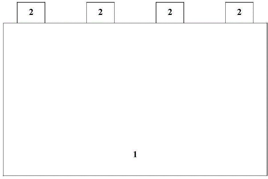
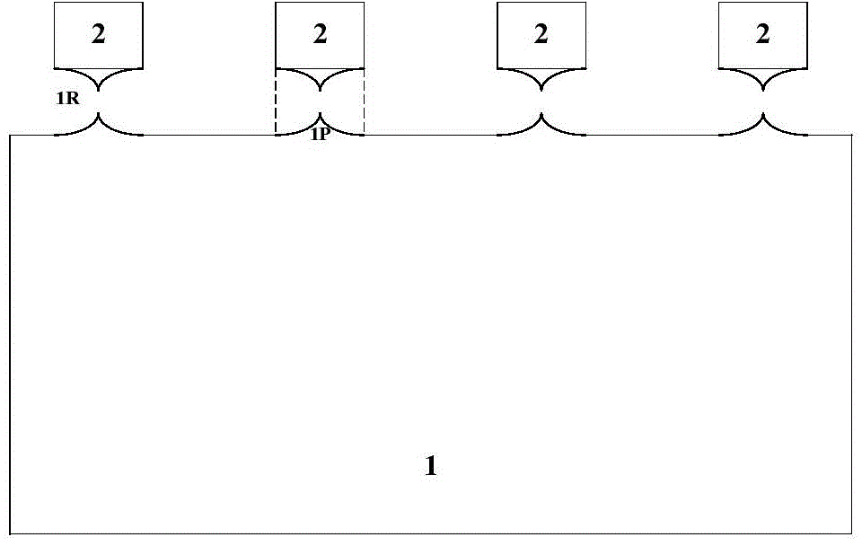
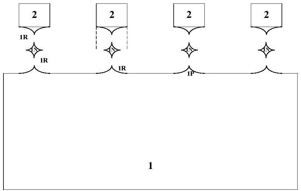
[0021] refer to Figure 7 as well as figure 1 , forming a hard mask pattern 2 on the substrate 1 . A substrate 1 is provided, which can be bulk Si, SOI, bulk Ge, GeOI, SiGe, GeSb, or a III-V or II-VI compound semiconductor substrate, such as GaAs, GaN, InP, InSb, etc. Wait. In order to be compatible with the existing CMOS process for application in the manufacture of large-s...
PUM
 Abstract
Description
Claims
Application Information
 - R&D
- Intellectual Property
- Life Sciences
- Materials
- Tech Scout
- Unparalleled Data Quality
- Higher Quality Content
- 60% Fewer Hallucinations
Browse by: Latest US Patents, China's latest patents, Technical Efficacy Thesaurus, Application Domain, Technology Topic, Popular Technical Reports.
© 2025 PatSnap. All rights reserved.Legal|Privacy policy|Modern Slavery Act Transparency Statement|Sitemap|About US| Contact US: help@patsnap.com