Preparation method for LED chip capable of forming light spots with specific planar geometric patterns through illumination, and structure of LED chip

A technology of LED chips and geometric figures, applied to electrical components, circuits, semiconductor devices, etc., can solve problems such as normal light intensity, uneven light distribution, and uneven spatial distribution of light

Active Publication Date: 2016-07-06
NANCHANG UNIV +1
View PDF3 Cites 8 Cited by
  • Summary
  • Abstract
  • Description
  • Claims
  • Application Information

AI Technical Summary

Problems solved by technology

For traditional front-mounted LED chips, the p-electrode and n-electrode are on the same side of the LED film and are located on the light-emitting surface. The light is emitted from the surroundings through the transparent substrate, and the front side is used to emit light from five sides. In this way, the spatial distribution of the emitted light is uneven. (The light spot is not good), the electrode blocks the light, and is located on the light-emitting surface, resulting in a relatively weak light intensity in the normal direction, mainly relying on the side light
For LED chips with a flip-chip struct

Method used


Image

  • Preparation method for LED chip capable of forming light spots with specific planar geometric patterns through illumination, and structure of LED chip
  • Preparation method for LED chip capable of forming light spots with specific planar geometric patterns through illumination, and structure of LED chip
  • Preparation method for LED chip capable of forming light spots with specific planar geometric patterns through illumination, and structure of LED chip

Examples


Embodiment Construction

[0053] The method and structure of an LED chip that irradiates light spots of a specific plane geometric pattern proposed by the present invention will be described in detail below with reference to the accompanying drawings and specific embodiments. It should be noted that the drawings of the present invention all adopt very simplified and inaccurate scales, which are only used to facilitate and clearly illustrate the present invention.

[0054] For ease of understanding, first briefly describe the whole process of preparing a LED chip with a vertical structure proposed by the present invention:

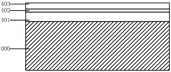
[0055] A. Grow gallium nitride-based LED thin films on the substrate material, that is, prepare epitaxial wafers;

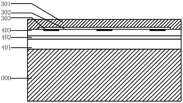
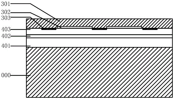
[0056] B. Prepare a complementary structure on the surface of the epitaxial wafer so that it corresponds to the n-electrode pattern or contains a specific plane geometry;

[0057] C. Depositing a reflective metal contact layer on the surface of the epitaxial...


PUM

PropertyMeasurementUnit
Thicknessaaaaaaaaaa
Thicknessaaaaaaaaaa
Thicknessaaaaaaaaaa

Abstract

The invention discloses a preparation method for an LED chip capable of forming light spots with specific planar geometric patterns through illumination, and a structure of the LED chip. The structure of the LED chip comprises a base plate layer, wherein the LED thin film on the growth substrate is transferred to the base plate layer; a complementary electrode layer, a reflective metal contact layer and a bonding protection layer are arranged between the base plate layer and the LED thin film from upper to lower in sequence; an n electrode is positioned on the LED thin film. Due to the complementary electrode layer, the shape design of the n electrode, and the differences of the metal reflectivity, the chip region (or a region without the complementary electrode layer) is high in luminance, wherein the chip region is corresponding to the reflective metal contact layer which is high in reflectivity and capable of forming ohmic contact with the LED thin film; the chip region (or a region with the complementary electrode layer) is low in luminance, wherein the chip region is corresponding to the bonding protection layer which is low in reflectivity and cannot form ohmic contact with the LED thin film easily, so that the LED chip can form the light spots with specific planar geometric patterns through illumination; and the planar geometric patterns are specific patterns or specific characters.

Description

technical field [0001] The invention relates to a semiconductor light-emitting device and a preparation method thereof, in particular to a preparation method and structure of an LED chip irradiating light spots of a specific plane geometric figure. Background technique [0002] Light-emitting diodes (LEDs) have been widely used in various lighting fields since their development, and are gradually becoming intelligent and diversified. In recent years, the light quality of LED lighting has been put forward higher requirements, especially in the fields of mobile lighting, entertainment lighting and other fields, there are diversified requirements for the light spots of LED chips. For example, a standard circular light spot in mobile lighting, a light spot with a special shape or containing various texts in entertainment lighting, etc. At present, the light spots that meet the above specific requirements are usually designed during the packaging or lamp manufacturing process. S...

Claims


Application Information

Patent Timeline
IPC IPC(8): H01L33/38H01L33/44H01L33/46H01L33/00
CPCH01L33/38H01L33/44H01L33/46H01L2933/0016H01L2933/0025
Inventor 王光绪江风益刘军林吴小明全知觉张建立
Owner NANCHANG UNIV
Why Eureka
Try Eureka