Chip packaging structure

A chip packaging structure and chip technology, applied in electrical components, electrical solid devices, circuits, etc., can solve the problems of low integration and anti-interference ability.

Inactive Publication Date: 2016-07-13
ZHUHAI JIELI TECH
View PDF3 Cites 2 Cited by
  • Summary
  • Abstract
  • Description
  • Claims
  • Application Information

AI Technical Summary

Problems solved by technology

[0003] Based on this, it is necessary to provide a chip packaging structure for the problems of low integra

Method used


Image

  • Chip packaging structure
  • Chip packaging structure
  • Chip packaging structure

Examples


Embodiment Construction

[0037] In order to make the technical solution of the present invention more clear, the technical solution of the present invention will be further described in detail below in conjunction with the accompanying drawings and specific embodiments.

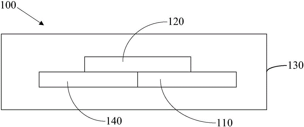
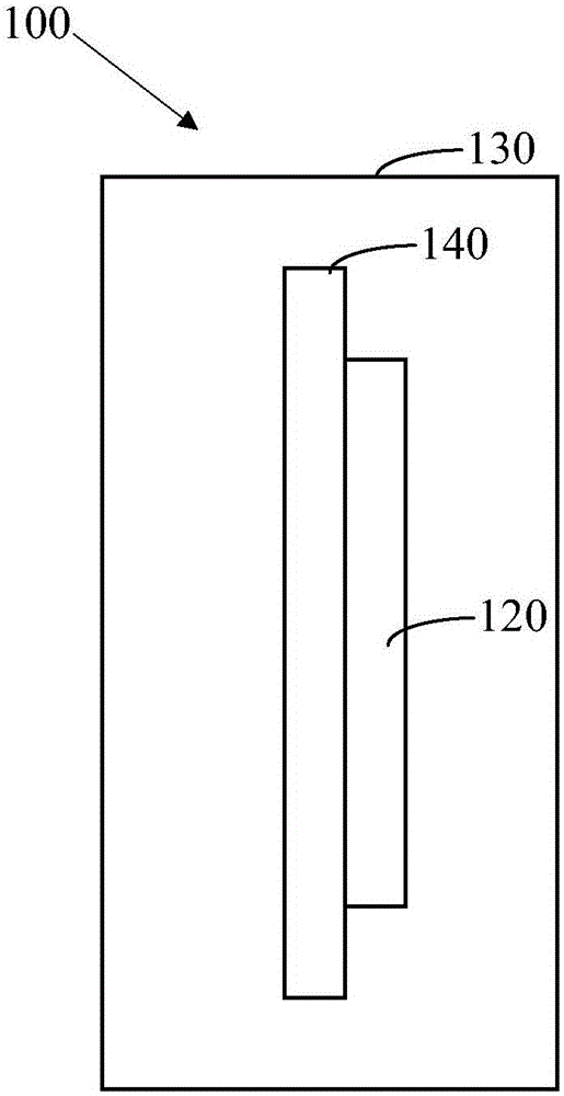
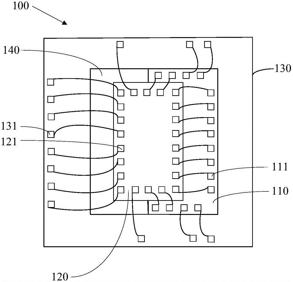
[0038] First of all, it should be noted that the first chip and the second chip mentioned in the present invention refer to various functional chips in the integrated circuit, such as: FLASH (flash memory) chip, SRAM (static random access memory) chip and DRAM (Dynamic Random Access Memory) chips, etc. No more examples here.

[0039] Wherein, both the first chip and the second chip have a circuit surface and a reverse surface opposite to the circuit surface. The circuit side refers to a side provided with a corresponding circuit layout. That is to say, the first chip in the present invention has a first circuit surface and a first reverse surface opposite to the first circuit surface. Correspondingly, the second chip has a second ...


PUM


Abstract

Disclosed in the invention is a chip packaging structure comprising a first chip, a second chip, an IC packaging shell, and a wafer made of a material having the same specification as that of the material employed by the first chip or the second chip. The first chip, the second chip, and the wafer are packaged into the IC packaging shell. A second reverse surface of the second chip is laminated on a first circuit surface of the first chip in a staggered mode. The wafer is adjacent to the first chip; and one surface, adjacent to the second chip, of the wafer and the first circuit surface of the first chip are located in a same plane and a second reverse surface that is not laminated on the first circuit surface is covered by the wafer. Because the second chip is stacked on the first chip in a staggered mode, the IC chip integration degree is improved effectively. Moreover, for a non-stacked area of the second chip and the first chip, the wafer made of the material having the same specification as that of the material employed by the first chip or the second chip is used for complete coverage and filling, so that working states of all function chips can be guaranteed effectively and thus a phenomenon that the performances are reduced or the power consumption is increased due to different materials can be avoided.

Description

technical field [0001] The invention relates to the technical field of integrated circuits, in particular to a chip packaging structure. Background technique [0002] At present, with the rapid growth of demand for miniaturized and portable consumer electronic products, the packaging requirements for integrated circuit IC chips are also getting higher and higher. Usually, traditional functional chips (such as: FLASH, SRAM or DRAM) are packaged separately. Then, after the packaging is completed, the manufacturer forms a system on the circuit board. However, the circuit system formed by using the traditional chip package structure has a low degree of integration and low anti-interference ability. Contents of the invention [0003] Based on this, it is necessary to provide a chip packaging structure for the problems of low integration and anti-interference ability of the circuit system formed by the traditional chip packaging structure. [0004] A chip packaging structure ...

Claims


Application Information

Patent Timeline
IPC IPC(8): H01L23/31H01L23/488
CPCH01L2224/05554H01L2224/48091H01L2224/48145H01L2924/00014H01L2924/00012H01L23/31H01L23/488
Inventor 张启明
Owner ZHUHAI JIELI TECH
Why Eureka
Try Eureka