OLED pixel arrangement structure and vapor-deposition mask of pixel arrangement structure

A pixel arrangement and pixel technology, which is applied in vacuum evaporation plating, sputtering plating, ion implantation plating, etc., can solve the problems of increasing the spacing of mask through holes, increasing the alignment space, and mask disconnection, etc. Reduce process difficulty, increase alignment space, and increase the effect of spacing

Inactive Publication Date: 2016-07-13
EVERDISPLAY OPTRONICS (SHANGHAI) CO LTD
View PDF4 Cites 6 Cited by
  • Summary
  • Abstract
  • Description
  • Claims
  • Application Information

AI Technical Summary

Problems solved by technology

[0003] The purpose of the present invention is to overcome the above-mentioned shortcomings in the prior art, and to provide a new pixel arrangement method to maximize the distance between pixels of different colors under high resolution and solve the problem of mask disconnection or At the same time, the pitch of the through holes of the mask is enlarged, the alignment space is increased, the difficulty of the process is reduced, and the occurrence of color mixing defects is avoided, thereby improving the product yield and reducing the production cost of the OLED pixel arrangement structure and the pixel arrangement structure. Evaporation mask

Method used


Image

  • OLED pixel arrangement structure and vapor-deposition mask of pixel arrangement structure
  • OLED pixel arrangement structure and vapor-deposition mask of pixel arrangement structure
  • OLED pixel arrangement structure and vapor-deposition mask of pixel arrangement structure

Examples


Embodiment Construction

[0021] In order to understand the technical content of the present invention more clearly, the following examples are given in detail.

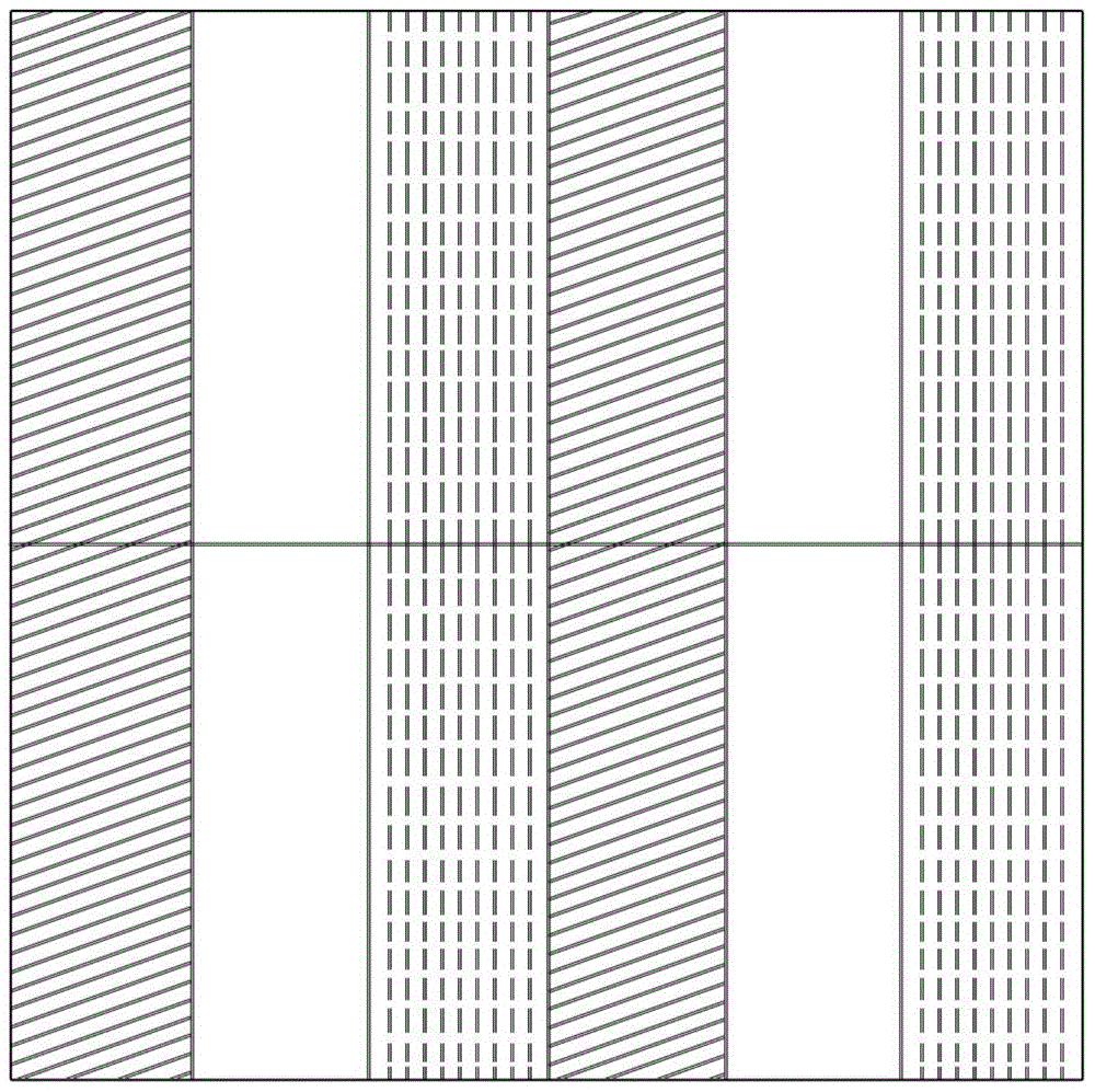
[0022] see Figure 4 , which is a schematic diagram of the pixel arrangement adopted by the OLED pixel arrangement structure of the present invention.

[0023] In one embodiment, the OLED pixel arrangement structure of the present invention can be formed as Figure 4 RGB pixel array shown. The pixel array includes: a plurality of first sub-pixel groups 5 composed of a plurality of first sub-pixels 2; a plurality of second sub-pixel groups 8 composed of second sub-pixels 3, composed of third sub-pixels 4 a plurality of third sub-pixel groups 9 . The first sub-pixel group 5 , the second sub-pixel group 8 and the third sub-pixel group 9 are arranged adjacently. Meanwhile, each first sub-pixel 2 is adjacent to a second sub-pixel 3 and a third sub-pixel 4 respectively, and each second sub-pixel 3 is adjacent to a first sub-pixel 2 and a third ...


PUM


Abstract

The invention relates to an OLED pixel arrangement structure and a vapor-deposition mask of the pixel arrangement structure, which belongs to the technical field of electronic equipment. RGB sub-pixels in the pixel array of the OLED pixel arrangement structure are hexagonal and are in a honeycomb distribution. One sub-pixel of any color in each pixel forms a same-color sub-pixel group together with two same-color sub-pixels just adjacent to the above sub-pixel. Based on the above novel pixel arrangement mode, the distance between different-color sub-pixels is maximized in the condition of high resolution. Therefore, the problem that the line of a mask is broken or the mask cannot be expanded can be solved. Based on the vapor-deposition mask, one through hole is shared by the same-color sub-pixel group, so that the spacing between the through holes of the mask is enlarged. Therefore, the alignment space is expanded, and the process difficulty is reduced. The occurrence of color-mixing defects is avoided. Furthermore, the product yield is improved and the production cost is lowered.

Description

technical field [0001] The present invention relates to the technical field of electronic equipment, in particular to the technical field of liquid crystal display panels, and specifically refers to an OLED pixel arrangement structure and an evaporation mask of the pixel arrangement structure. Background technique [0002] The pixels of traditional displays use such as figure 1 In the shown RGB sidebyside arrangement, the sub-pixels RGB are arranged sequentially in the horizontal direction. At high resolution, because the pixels of the same color are too close together, such as image 3 In the manufacture of the OLED mask (shadowmask) shown, there may be problems of disconnection L or failure to open the net. At the same time, if figure 2 and image 3 As shown, because the distances between different colors are very close, the alignment space S is limited, the technical process is difficult, and color mixing defects are prone to occur during the production of panel evap...

Claims


Application Information

Patent Timeline
Patent Type & Authority Applications(China)
IPC IPC(8): H01L27/32C23C14/04
Inventor 吴界煌
Owner EVERDISPLAY OPTRONICS (SHANGHAI) CO LTD
Why Eureka
Try Eureka