360-degree light emitting LED device and 360-degree light emitting LED light source

A technology of LED devices and LED chips, which is applied in the direction of semiconductor devices, electric solid devices, electrical components, etc., can solve problems such as high thermal resistance, difficult control of product quality, difficulty in selection, use and processing of light conversion layers, and achieve product quality. High, easy to manufacture and material selection effect

Active Publication Date: 2016-07-20
苏州汇杰紫芯光电有限公司
View PDF6 Cites 6 Cited by
  • Summary
  • Abstract
  • Description
  • Claims
  • Application Information

AI Technical Summary

Problems solved by technology

The existing LED filaments have the following problems: First, the heat dissipation is not enough, which leads to the brightness of the filaments being easily attenuated, because the chip structure and only insulating glue for heat conduction will produce high thermal resistance, low thermal conductivity, and the bottom substrate area is limited and difficult to dissipate heat ; Second, the reliability of the gold wire is low. Gold wires are used for electrical interconnection between the formal LED chips. When the filament is repeatedly powered on and off, it will alternate between hot and cold. broken, resulting in filament failure
This structure realizes light emission from both sides, which effectively increases the light emission area, but the side light emission effect is not good, and 360-degree light emission cannot be achieved.
Not only that, this type of structure directly makes circuits on the light conversion layer, the selection, use and processing of the light conversion layer are relatively difficult, and it is easy to affect the light conversion performance of the light conversion layer, making product quality difficult to control

Method used


Image

  • 360-degree light emitting LED device and 360-degree light emitting LED light source
  • 360-degree light emitting LED device and 360-degree light emitting LED light source
  • 360-degree light emitting LED device and 360-degree light emitting LED light source

Examples


Embodiment 1

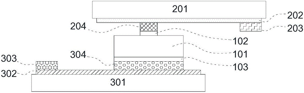
[0049] This embodiment is a typical scheme of single LED chip packaging, its structure is as follows image 3 Shown:

[0050] The LED chip 101 is a blue light LED chip with a vertical structure, and its luminous wavelength range is 440-470nm. The chip N electrode 102 and the chip P electrode 103 are respectively located at the upper and lower ends of the LED chip 101. The main material of the chip P electrode 103 is ITO transparent and conductive film. It should be noted that this embodiment schematically illustrates the situation of blue LED chips, and the present invention also includes various types of LED chips such as red light and green light, which are all equivalent protection scopes of the present invention.

[0051] Wherein, the main material of the transparent upper substrate 201 is sapphire, and a patterned first transparent conductive layer 202 is arranged on one surface thereof, and the main material of the first transparent conductive layer 202 is a graphene tr...

Embodiment 2

[0061] like Figure 4 As shown, this embodiment is another typical scheme of packaging a single LED chip. Its structure is as Figure 4 As shown, the difference between this embodiment and Embodiment 1 is that the first external electrode 203 and the second external electrode 303 are improved:

[0062] The first external electrode 203 is changed to directly make a long first conductive circuit layer 205 on the transparent upper substrate 201 to connect with the first transparent conductive layer 202, and the first conductive circuit layer 205 acts as an external electrode and enhances electrical and thermal conductivity. The role of ability.

[0063] Similarly, the second external electrode 303 is changed to directly make a long second conductive line layer 305 on the transparent lower substrate 301 to connect with the second transparent conductive layer 302, and the second conductive line layer 305 acts as an external electrode and enhances The role of electrical and therm...

Embodiment 3

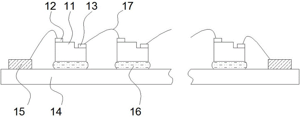
[0066] like Figure 5 As shown, this embodiment discloses that multiple LED chips are connected in series, and wrapped and packaged with fluorescent glue, so as to form an LED filament that can emit white light.

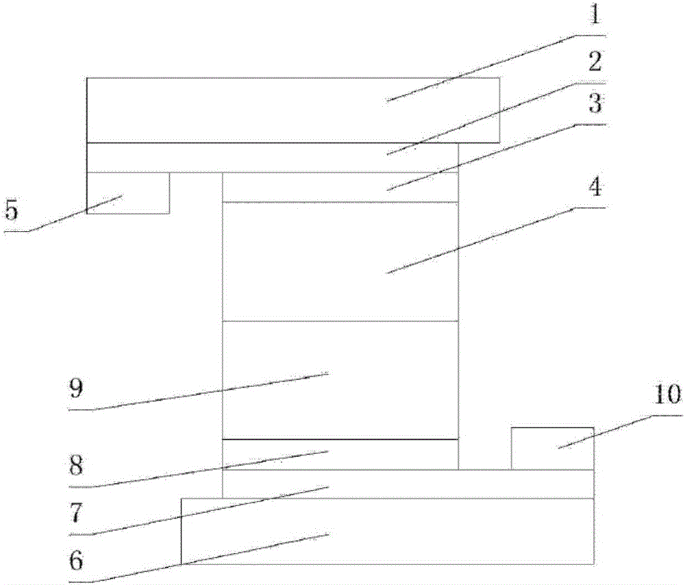
[0067] Figure 5 is a schematic diagram of the LED packaging structure of this embodiment, Image 6 It is a schematic structural diagram of the separation of the upper and lower transparent substrates, and its structure is similar to that of Embodiment 1, except that:

[0068] The number of LED chips 101 is 5, wherein the N electrodes 102 of two chips face the transparent upper substrate 201, and the N electrodes 102 of the other three chips face the transparent lower substrate 301, and the LED chips 101 of different orientations are arranged at intervals; The main material of the substrate 201 is transparent ceramics, a patterned first transparent conductive layer 202 is arranged on one surface, and a first conductive circuit layer 205 is also arranged on the same...


PUM


Abstract

The present invention in particular discloses a 360-degree light emitting LED device and a 360-degree light emitting LED light source. The LED device comprises an LED chip, the LED chip has a vertical structure, and the upper and lower ends of the LED chip are equipped with an N electrode and a P electrode respectively. The LED device also comprises a transparent upper substrate and a transparent lower substrate, and the LED chip is fixed between the transparent upper substrate and the transparent lower substrate. A first transparent conductive layer is arranged on the surface of the transparent upper substrate opposite to the LED chip, is electrically connected with the N electrode of the LED chip and leads out the N electrode to a first external electrode, a second transparent conductive layer is arranged on the surface of the transparent lower substrate opposite to the LED chip, is electrically connected with the P electrode of the LED chip and leads out the P electrode to a second external electrode, and a light conversion material layer wraps the transparent upper substrate, the transparent lower substrate and the LED chip. The LED device and the LED light source of the present invention can emit light 360 degrees, and are lower in production difficulty and higher in product quality.

Description

technical field [0001] The invention belongs to the technical field of LEDs, and in particular relates to a 360-degree light-emitting LED device and an LED light source. Background technique [0002] LED has the advantages of small size, low driving voltage, high luminous efficiency, and long life. It has been used in many lighting and decorative products, especially in the replacement of traditional lighting sources, to achieve 360 ​​full-angle light sources. Light distribution design is of great significance. The existing 360-degree luminous products mainly have two realization methods: one is LED filament, and the other is pasted on a special-shaped PCB with SMD LEDs. Through the combination and arrangement of PCBs, 360-degree luminescence can be realized. [0003] like figure 1 Shown is the structure of the existing LED filament, all of which use insulating glue 16 to fix multiple LED chips 11 on the substrate 14, and the P electrodes 12 of the LED chips and the N elec...

Claims


Application Information

Patent Timeline
IPC IPC(8): H01L25/075H01L33/48H01L33/50H01L33/62
CPCH01L25/0753H01L33/48H01L33/50H01L33/62H01L2224/48091H01L2224/48137H01L2224/49107H01L2224/73253H01L2224/73265H01L2924/00014
Inventor 李正豪陈海英许朝军
Owner 苏州汇杰紫芯光电有限公司
Why Eureka
Try Eureka