Dual gate line array substrate, testing method, display panel and display device

A technology of array substrates and double gate lines, which is applied in semiconductor/solid-state device testing/measurement, electrical components, electric solid-state devices, etc., can solve problems such as defective pixels, undetectable, cost increases, etc., and improve the detection rate of pixels , Improve product quality control, improve the effect of product quality

Active Publication Date: 2016-07-20
BOE TECH GRP CO LTD +1
View PDF7 Cites 13 Cited by
  • Summary
  • Abstract
  • Description
  • Claims
  • Application Information

AI Technical Summary

Problems solved by technology

[0006] However, in the array test (ArrayTest) of the double-grid line array substrate, the existing double-grid line array substrate often leads to the problem of low pixel detection rate, resulting in low product quality control, which in turn leads to an increase in related costs
For example, pixel defects caused by indium tin oxide (ITO) residues are a phenomenon encountered in the production process of double grid line array substrates
However, in the array test of the prior art dual grid line array substrate, in some cases, it may not be possible to detect the defective pixel caused by the residual conductive material.

Method used


Image

  • Dual gate line array substrate, testing method, display panel and display device
  • Dual gate line array substrate, testing method, display panel and display device
  • Dual gate line array substrate, testing method, display panel and display device

Examples


Embodiment Construction

[0033] Embodiments of the present disclosure are described below with reference to the accompanying drawings. In the following description, numerous specific details are set forth in order to enable those skilled in the art to more fully understand and practice the present disclosure. It will be apparent, however, to one skilled in the art that the present disclosure may be practiced without some of these specific details. Furthermore, it should be understood that the disclosure is not limited to the particular embodiments described. Rather, it is conceivable to implement the present disclosure in any combination of the features and elements described below, regardless of whether they relate to different embodiments. Accordingly, the following aspects, features, embodiments and advantages are by way of illustration only and should not be considered elements or limitations of the claims unless explicitly stated in the claims.

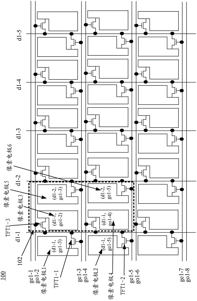
[0034] As used herein, a gate line including "ge...


PUM


Abstract

The invention discloses a dual gate line array substrate. In two pixel pairs in a limited area between any group of dual gate lines and adjacent two groups of dual gate lines and adjacent two data lines, pixel units in each pixel pair are respectively connected with the same data line in the adjacent two data lines, and adjacent two pixel units in two pixel pairs in the data line extending direction are connected with different data lines in adjacent two data lines respectively; in adjacent two pixel pairs in the extending direction of any group of dual gate lines, data lines connected with two pixel units in one pixel pair and data lines connected with two pixel units in the other pixel pair are different but adjacent; and adjacent two pixel units in the data line extending direction are respectively connected with adjacent gate lines with different transmission and scanning signals, and adjacent two pixel units in the extending direction of any group of dual gate lines are respectively connected with adjacent gate lines with different transmission and scanning signals. The dual gate line array substrate can improve the pixel detection rate.

Description

technical field [0001] Embodiments of the present disclosure relate to the display field, and more specifically, to a double grid line array substrate, a testing method, a display panel and a display device. Background technique [0002] Generally speaking, display devices can be classified into cathode ray tube display CRT, plasma display PDP, liquid crystal display LCD, light emitting diode LED display, active light emitting diode OLED display, etc. according to different manufacturing materials, for example. At present, flat panel displays such as LCD and LED displays have gradually replaced traditional displays such as CRT, are widely used in various industries, and become an indispensable component of most electronic devices. [0003] In displays such as LCD and LED displays, an array substrate is a major component. In the array substrate, pixel units are arranged periodically. Each pixel unit may include a thin film transistor (TFT) and a pixel electrode, and each pi...

Claims


Application Information

Patent Timeline
Patent Type & Authority Applications(China)
IPC IPC(8): H01L27/12H01L21/66
CPCH01L22/30H01L27/1214H01L27/1248G09G2300/0426G09G2330/10G09G3/006H01L27/1244H01L27/12H10K19/10G01R31/2815H01L27/124H01L27/1259H01L29/78648
Inventor 任兴凤
Owner BOE TECH GRP CO LTD
Why Eureka
Try Eureka