

Electromagnetic wave shielding material, and method for manufacturing same
a technology shielding material, which is applied in the direction of paper/cardboard containers, transportation and packaging, synthetic resin layered products, etc., to achieve the effects of reducing the treatment cost of electromagnetic shielding material, high speed, and suppressing the cost of equipmen
- Summary
- Abstract
- Description
- Claims
- Application Information
AI Technical Summary
Benefits of technology
Problems solved by technology
Method used
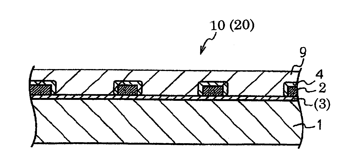
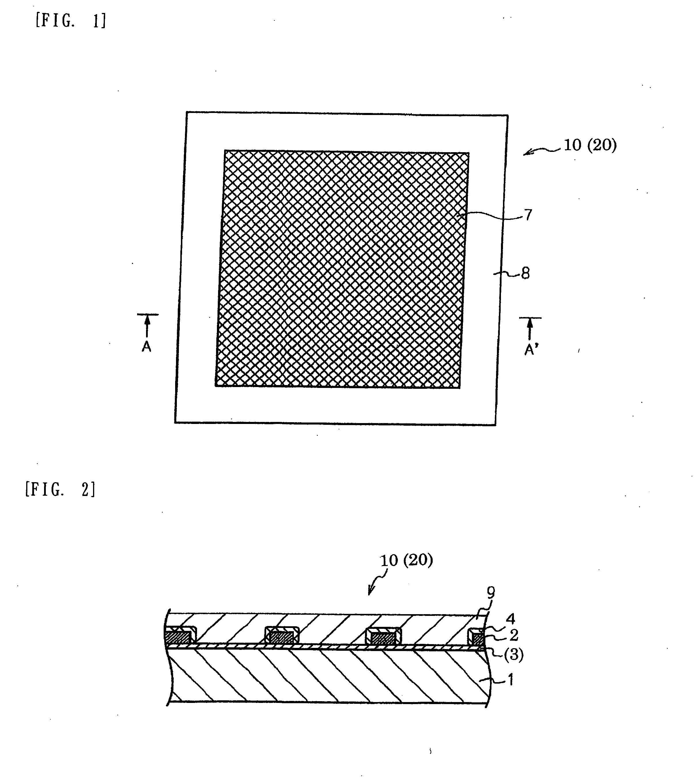
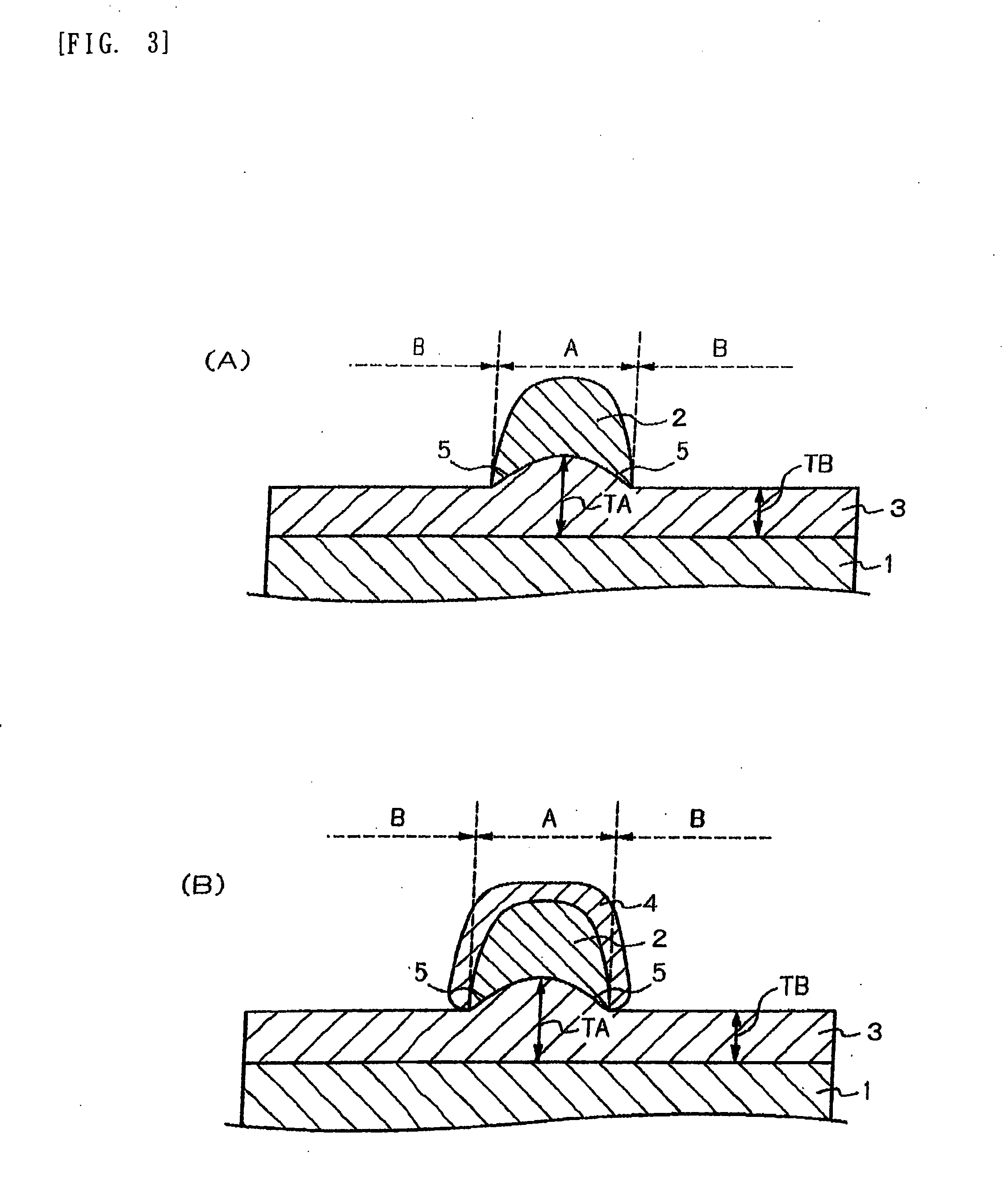
Image

Examples
example 1
[0291]The present Example is a working example related to the invention of the electromagnetic wave shielding material of the second embodiment.
[Preparation of Intaglio]
[0292]First of all, a gravure printing plate cylinder having a printing plate depth of 12 μm, which is a mesh pattern in a regular lattice shape having a line width of 17 μm and a line pitch of 270 μm, was prepared as the intaglio roll 62.
[Preparation of Transparent Substrate]
[0293]Subsequently, a longitudinal rolled, biaxially stretched transparent polyethylene terephthalate (PET) film, on one surface of which had been subjected to an easy adhesion treatment by coating a polyester resin based easily adhesive layer, having a width of 1,000 mm and a thickness of 100 μm was used as the transparent substrate 1. Also, a composition having 12 parts by mass of an epoxy acrylate prepolymer, 44 parts by mass of a monofunctional monomer composed of phenoxyethyl acrylate and 9 parts by mass of a trifunctional monomer composed ...
experimental example 1
[0300]For the purpose of confirming any influence of the acid concentration in the electrical resistance reducing treatment, the untreated sample of the electromagnetic wave shielding material obtained in Example 1 was treated in the same manner as in Example 1 by dipping in an acid treatment tank composed of a hydrochloric acid aqueous solution at 40° C. for 30 seconds, drawing up and rinsing with water at 20° C., followed by drying the moisture, except for changing the concentration of the hydrochloric acid aqueous solution to from 0.5% by mass to 15% by mass. A surface resistivity of the obtained samples was not influenced by the hydrochloric acid concentration and found to be about 0.8Ω / □ in all of the samples. A result of this Experimental Example is shown in FIG. 12.
examples 2 to 6
[0301]In Example 1, the electrical resistance reducing treatment was carried out in the same manner as in Example 1, except for dipping each sample after the acid treatment for seconds while regulating the warm water treatment temperature to 22° C. (Example 2), 40° C. (Example 3), 50° C. (Example 4), 70° C. (Example 5) and 90° C. (Example 6), respectively. A relation between the warm water temperature and the surface resistivity (value) (Examples 2 to 6) is shown in FIG. 13.
[0302]It was confirmed that the surface resistivity is remarkably lowered with an elevation of the warm water temperature. In this respect, though Example 6 is the same condition as Example 1 with respect to the water temperature of 90° C., it was provided as a series for the purpose of also evaluating the reproducibility. In Example 6, the surface resistivity is 0.56Ω / □, a value of which is increased as compared with Example 1; however, it may be determined that this falls with an experimental error range.
PUM
| Property | Measurement | Unit |
|---|---|---|
| width | aaaaa | aaaaa |
| temperature | aaaaa | aaaaa |
| RH | aaaaa | aaaaa |
Abstract
Description
Claims
Application Information