High-voltage semiconductor device and manufacturing method thereof

A manufacturing method and semiconductor technology, applied in the direction of semiconductor devices, electrical components, circuits, etc., can solve the problems of increasing the on-resistance of transistors in the size of the chip area, increasing the on-resistance of transistors, increasing the performance of P-type high-voltage semiconductor devices, etc. Effect of on-resistance

Active Publication Date: 2019-01-04
VANGUARD INTERNATIONAL SEMICONDUCTOR CORPORATION
View PDF4 Cites 0 Cited by
  • Summary
  • Abstract
  • Description
  • Claims
  • Application Information

AI Technical Summary

Problems solved by technology

However, this will increase the size of the device, increase the chip area and increase the on-resistance (Ron) of the transistor.
Furthermore, since the mobility of holes (holes) is lower than that of electrons, the on-resistance of the P-type high-voltage semiconductor device will be higher than that of the N-type high-voltage semiconductor device, which is not conducive to the P-type high-voltage semiconductor device. performance improvement

Method used


Image

  • High-voltage semiconductor device and manufacturing method thereof
  • High-voltage semiconductor device and manufacturing method thereof
  • High-voltage semiconductor device and manufacturing method thereof

Examples


Embodiment Construction

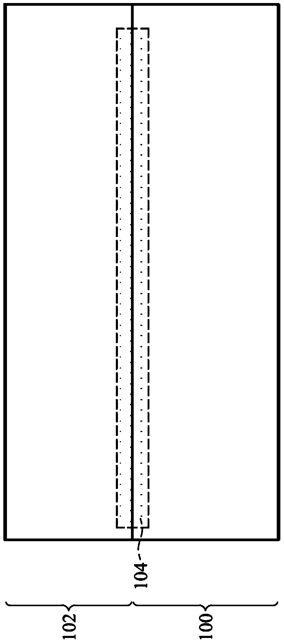
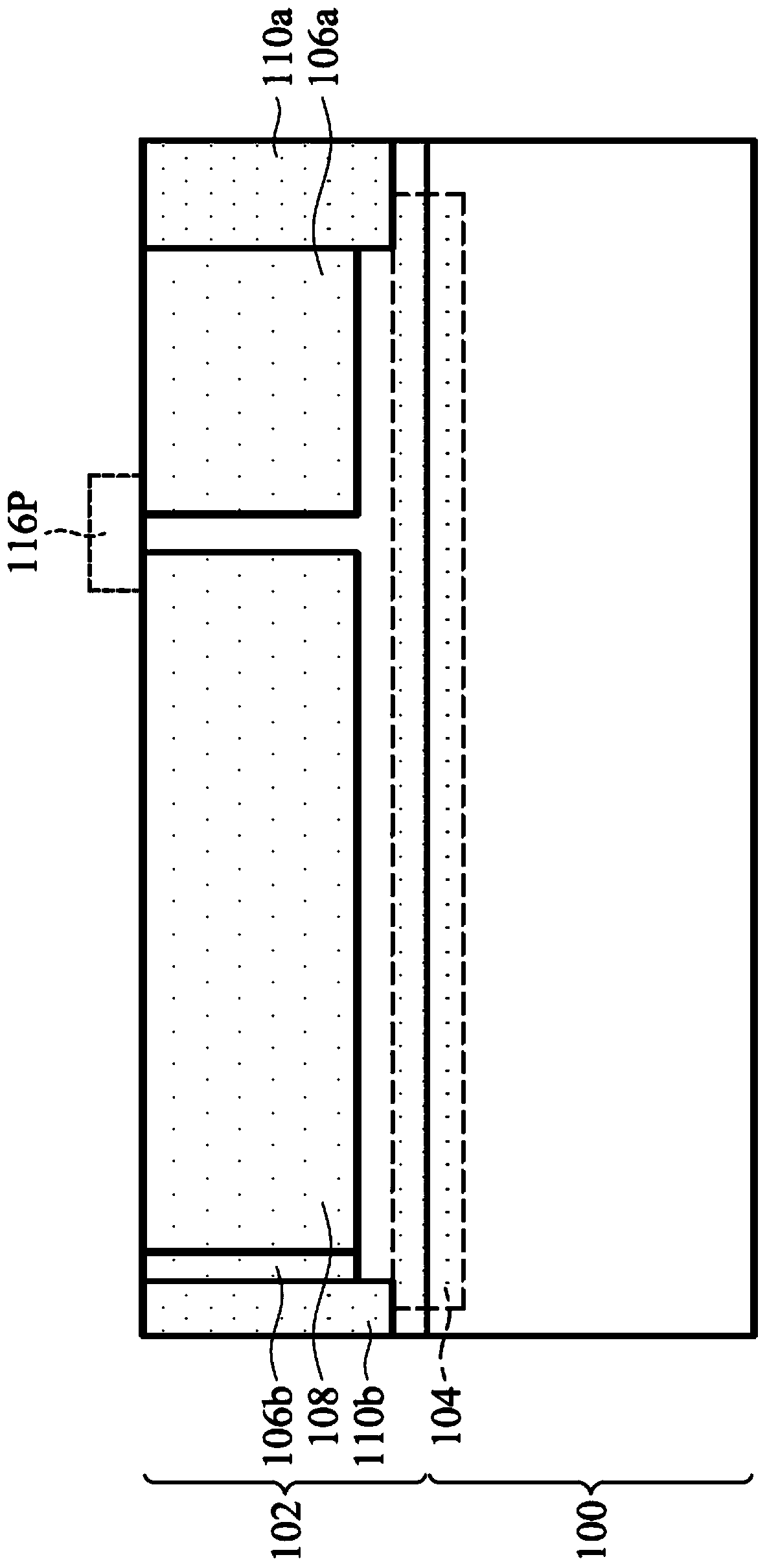
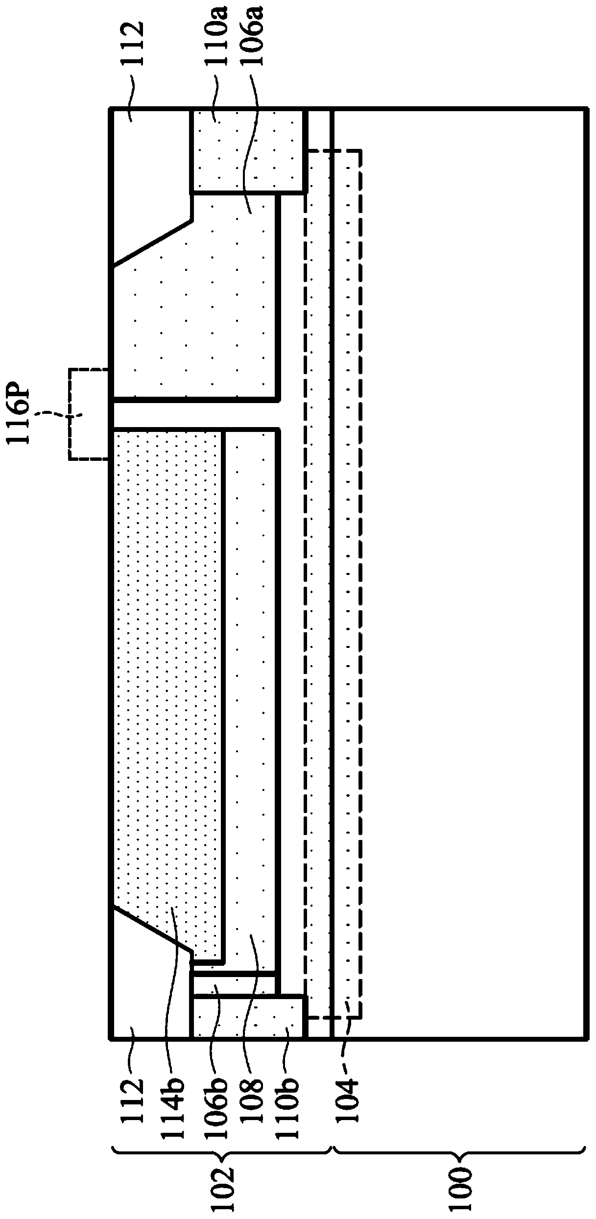
[0048] The high-voltage semiconductor device of the present invention will be described in detail below. It should be appreciated that the following description provides many different embodiments or examples for implementing different aspects of the invention. The specific elements and arrangements described below are intended to briefly describe the invention. Of course, these are only used as examples rather than limitations of the present invention. Furthermore, repeated reference numbers or designations may be used in different embodiments. These repetitions are for simplicity and clarity of description of the present invention and do not represent any association between the different embodiments and / or structures discussed. Furthermore, when it is mentioned that a first material layer is located on or above a second material layer, it includes the situation that the first material layer and the second material layer are in direct contact. Alternatively, one or more l...


PUM


Abstract

The invention provides a high-voltage semiconductor device and a manufacturing method thereof. The high-voltage semiconductor device comprises a substrate, an epitaxial layer, a gate structure, a first conductive type high-voltage well region, a second conductive type high-voltage well region, a source region, a drain region and a stack structure, wherein the epitaxial layer is arranged on the substrate and has a first conductive type; the gate structure is arranged on the epitaxial layer; the first conductive type high-voltage well region and the second conductive type high-voltage well region are arranged in the epitaxial layer at two sides of the gate structure respectively; the first conductive type is different from the second conductive type; the source region and the drain region are arranged in the epitaxial layer at two sides of the gate structure; the stack structure is arranged between the gate structure and the drain region and comprises a barrier layer, an insulating layer and a conductive layer; the insulating layer is arranged on the barrier layer; and the conductive layer is arranged on the insulating layer and is electrically connected with the source region or the gate structure. Through the gate structure comprising the conductive layer, the electric field intensity of a channel in the epitaxial layer can be reduced, so that the on-resistance of the high-voltage semiconductor device is reduced.

Description

technical field [0001] The present invention relates to a semiconductor device and a method of fabricating the same, and more particularly, to a high-voltage semiconductor device and a method of fabricating the same. Background technique [0002] High-voltage semiconductor device technology is suitable for high-voltage and high-power integrated circuits. Conventional high-voltage semiconductor devices, such as vertically diffused metal oxide semiconductor (VDMOS) transistors and horizontally diffused metal oxide semiconductor (LDMOS) transistors, are mainly used in device applications above 18V. The advantages of high-voltage device technology are that it is cost-effective and easily compatible with other manufacturing processes. It has been widely used in display driver IC components, power supplies, power management, communications, automotive electronics or industrial control. [0003] High voltage semiconductor devices use the gate voltage to create the channel and cont...

Claims


Application Information

Patent Timeline
Patent Type & Authority Patents(China)
IPC IPC(8): H01L29/43H01L21/28
Inventor 罗宗仁刘兴潮陈巨峰周苇俊
Owner VANGUARD INTERNATIONAL SEMICONDUCTOR CORPORATION
Why Eureka
Try Eureka