Semiconductor device and manufacturing method for same

a technology of semiconductor devices and semiconductors, applied in semiconductor devices, semiconductor/solid-state device details, electrical apparatus, etc., can solve the problems of thin insulating layer reducing insulation properties, and achieve the effects of reducing the density of electric fields, improving insulation properties, and high insulation properties

Active Publication Date: 2018-05-22
MITSUBISHI ELECTRIC CORP
View PDF26 Cites 0 Cited by
  • Summary
  • Abstract
  • Description
  • Claims
  • Application Information

AI Technical Summary

Benefits of technology

[0011]In the semiconductor device according to the first aspect of the present invention, an electric field concentrated place in the heat spreader is distributed to a plurality of electric field concentrated places by the chamfered portion located at the outer peripheral end portion of the back surface of the heat spreader, to thereby reduce a density of the electric fields, and thus insulation properties can be improved. As a result, the semiconductor device having high insulation properties can be obtained even in a case where it is feared that a temperature rise or the like during an operation of the semiconductor element causes the insulating layer to reduce the insulation properties.
[0012]Moreover, the insulating sheet portion is formed so as to have the same plane, so that R obtained by the R chamfering or C obtained by the C chamfering is set to a dimension that does not interfere with filling the space region with the molding resin to form the chamfered portion, which allows the space region between the chamfered portion and the insulating sheet portion (insulating layer) to be filled with the molding resin. As a result, the semiconductor device having excellent heat dissipation characteristics and excellent insulation properties can be obtained at a relatively low cost.
[0013]The semiconductor device according to the second aspect of the present invention has the structure without the space region between the insulating sheet portion and the chamfered portion by closely bonding the bent portion of the insulating sheet portion to the chamfered portion of the heat spreader, to thereby eliminate room for voids formed in the space region, the voids being a factor in electric discharge. This can reduce a heat resistance between the heat spreader and the molding resin and improve the insulation properties.

Problems solved by technology

An insulating layer located below the power chips is preferably thin to increase heat dissipation characteristics, but it is feared that the thin insulating layer reduces the insulation properties.

Method used


Image

  • Semiconductor device and manufacturing method for same
  • Semiconductor device and manufacturing method for same
  • Semiconductor device and manufacturing method for same

Examples


first embodiment

[0040](Structure)

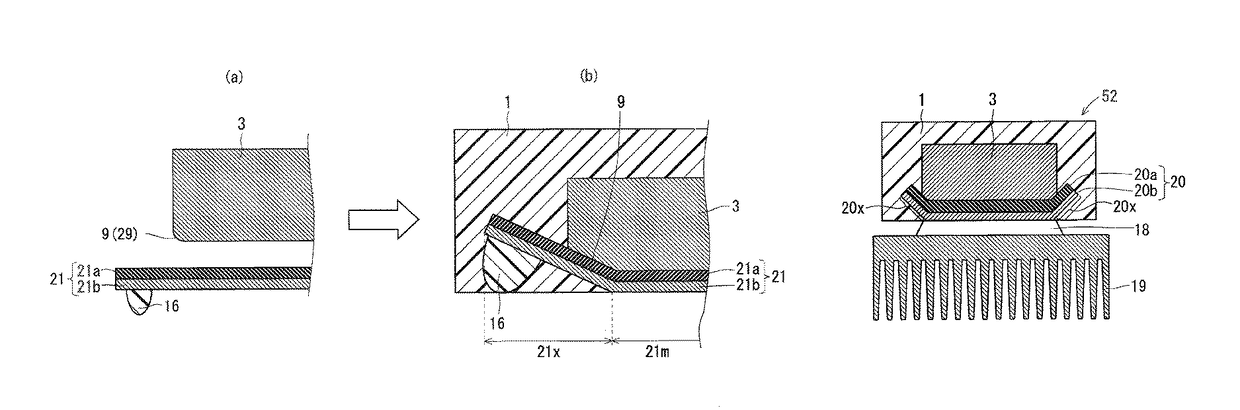
[0041]FIG. 1 is an explanatory diagram showing a structure of a semiconductor device 51 being a first embodiment of the present invention. Part (a) of FIG. 1 is a cross-sectional view showing a cross-sectional structure, and part (b) of FIG. 1 is a plan view showing a planar structure. In addition, parts (a), (b) of FIG. 1 are each provided with the XYZ Cartesian coordinate system.

[0042]As shown in FIG. 1, a plurality of (two) power elements 4 formed into chips are mounted on a surface of a heat spreader 3 with a solder 28 therebetween. Aluminum wires 5 are connected between the plurality of power elements 4 and between the power elements 4 and signal terminals 6. A material for the heat spreader 3 is preferably metals such as aluminum and copper that are easily processed and have a high thermal conductivity.

[0043]An insulating sheet portion 2 is located on a back surface side of the heat spreader 3. The insulating sheet portion 2 has a laminated structure of an ins...

second embodiment

[0074](Structure)

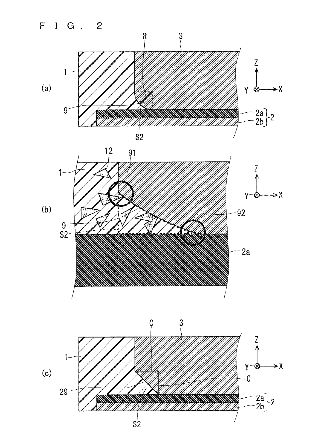
[0075]FIG. 4 is an explanatory diagram schematically showing a surrounding structure of a chamfered portion of a heat spreader 3 in a semiconductor device 52 being a second embodiment. A structure shown in part (a) of FIG. 4 corresponds to the focused region A1 in the semiconductor device 51 shown in FIG. 1, and a structure shown in part (b) of FIG. 4 is an enlarged diagram of a focused region in part (a) of FIG. 4.

[0076]As shown in FIG. 4, an insulating sheet portion 20 is located on a back surface side of the heat spreader 3. The insulating sheet portion 20 has a laminated structure of an insulating layer 20a and a metal foil 20b (metal layer), and a surface of the insulating layer 20a is closely bonded to the back surface of the heat spreader 3 having a sagging surface 9. The insulating layer 20a has a thermal conductivity higher than that of a molding resin 1 and has high insulation properties.

[0077]In this manner, the insulating sheet portion 20 has a main body...


PUM


Abstract

In the present invention, a heat spreader has a sagging surface or a C surface being a chamfered portion at an outer peripheral end portion of a back surface thereof. A plurality of power elements formed into chips are mounted on a surface of the heat spreader with a solder therebetween, and an insulating sheet portion is located on the back surface side of the heat spreader. The insulating sheet portion has a laminated structure of an insulating layer and a metal foil, and the insulating layer being the upper layer is closely bonded to the back surface of the heat spreader. A space region between the sagging surface and the insulating sheet portion is filled with a molding resin.

Description

TECHNICAL FIELD[0001]The present invention relates to a semiconductor device sealed with resin and a method for manufacturing the semiconductor device, and more particularly, to a semiconductor device including an insulating layer having a thermal conductivity higher than that of a sealing resin and a method for manufacturing the semiconductor device.BACKGROUND ART[0002]It is extremely important that power semiconductor devices keep high insulation properties while efficiently dissipating heat generated by power chips to the outside. An insulating layer located below the power chips is preferably thin to increase heat dissipation characteristics, but it is feared that the thin insulating layer reduces the insulation properties.[0003]Moreover, the power semiconductor devices often adopt semiconductor devices having a resin-sealed structure entirely full-molded with one type of resin. For example, Patent Document 1 discloses a semiconductor module as a semiconductor device having a re...

Claims


Application Information

Patent Timeline
Patent Type & Authority Patents(United States)
IPC IPC(8): H01L23/367H01L21/48H01L23/433H01L23/16H01L23/373H01L23/31H01L21/56
CPCH01L23/3675H01L21/4878H01L23/4334H01L23/433H01L21/4882H01L21/565H01L23/16H01L23/3107H01L23/3735H01L2924/181H01L2224/73265H01L2224/49175H01L2224/49111H01L2224/49109H01L2224/48247H01L2224/48139H01L2224/48137H01L2224/48091H01L23/367H01L2924/00H01L2924/00014H01L2924/00012
Inventor SAKAMOTO, KEN
Owner MITSUBISHI ELECTRIC CORP
Why Eureka
Try Eureka