Semiconductor device and manufacturing method thereof

A manufacturing method and semiconductor technology, which are used in semiconductor/solid-state device manufacturing, semiconductor devices, electric solid-state devices, etc., can solve the problems of high substrate cost, difficult threshold voltage control, and inability to meet the breakdown voltage requirements of different devices at the same time. , to achieve the effect of increasing the breakdown voltage and reducing the electric field density

Pending Publication Date: 2022-04-29
WUHAN XINXIN SEMICON MFG CO LTD
View PDF0 Cites 0 Cited by
  • Summary
  • Abstract
  • Description
  • Claims
  • Application Information

AI Technical Summary

Problems solved by technology

[0002] The semiconductor-on-insulator (SOI) structure includes a lower substrate, an insulating buried layer and an upper semiconductor layer. The SOI substrate is divided into partially depleted SOI (Partially-Depleted Semiconductor-On-Insulator, PDSOI) and fully depleted according to whether the active region is depleted. Depleted SOI (Fully-Depleted Semiconductor-On-Insulator, FDSOI), generally speaking, the upper semiconductor layer of the FDSOI substrate will be relatively thin, and the cost of the substrate is relatively high. On the other hand, the threshold voltage of FDSOI is not easy to control. The PDSOI substrate is still used, wherein the thickness of the upper semiconductor layer of the PDSOI substrate purchased from the manufacturer is equal, but in the process of manufacturing semiconductor devices, different devices may need to be fabricated on the same substrate. Different devices have different requirements for breakdown voltage, and the use of upper semiconductor layers with equal thickness cannot meet the requirements of different devices for breakdown voltage at the same time.

Method used


Image

  • Semiconductor device and manufacturing method thereof
  • Semiconductor device and manufacturing method thereof
  • Semiconductor device and manufacturing method thereof

Examples


Embodiment Construction

[0049] In order to make the purpose, advantages and features of the present invention clearer, the semiconductor device and its manufacturing method proposed by the present invention will be further described in detail below with reference to the accompanying drawings. It should be noted that all the drawings are in a very simplified form and use imprecise scales, and are only used to facilitate and clearly assist the purpose of illustrating the embodiments of the present invention.

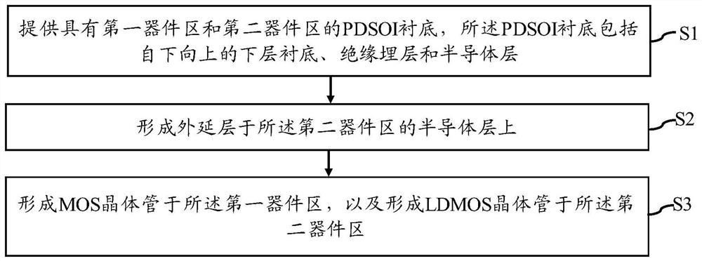
[0050] An embodiment of the present invention provides a method for manufacturing a semiconductor device, see figure 1 , figure 1 It is a flowchart of a method for manufacturing a semiconductor device according to an embodiment of the present invention, and the method for manufacturing a semiconductor device includes:

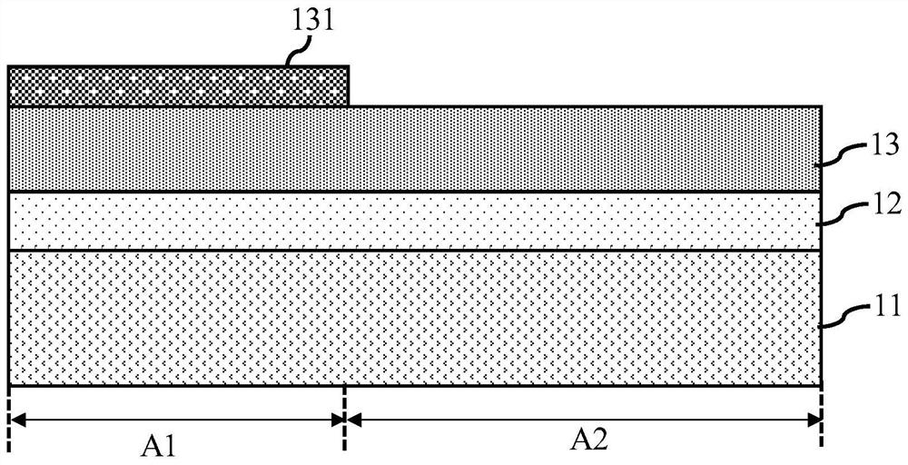
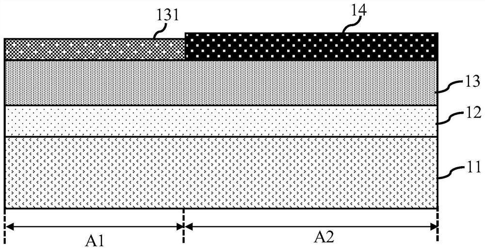
[0051] Step S1, providing a PDSOI substrate having a first device region and a second device region, the PDSOI substrate comprising an underlying substrate, an insulating buried ...


PUM

PropertyMeasurementUnit
relative permittivityaaaaaaaaaa

Abstract

The invention provides a semiconductor device and a manufacturing method thereof, and the method comprises the steps: providing a PDSOI substrate with a first device region and a second device region, and the PDSOI substrate comprises a lower substrate, an insulating buried layer and a semiconductor layer from bottom to top; forming an epitaxial layer on the semiconductor layer of the second device region; forming an MOS (Metal Oxide Semiconductor) transistor in the first device region and forming an LDMOS (Laterally Diffused Metal Oxide Semiconductor) transistor in the second device region. According to the invention, the breakdown voltage of the LDMOS transistor can be improved.

Description

technical field [0001] The invention relates to the field of semiconductor integrated circuit manufacturing, in particular to a semiconductor device and a manufacturing method thereof. Background technique [0002] The semiconductor-on-insulator (SOI) structure includes a lower substrate, an insulating buried layer and an upper semiconductor layer. The SOI substrate is divided into partially depleted SOI (Partially-Depleted Semiconductor-On-Insulator, PDSOI) and fully depleted according to whether the active region is depleted. Depleted SOI (Fully-Depleted Semiconductor-On-Insulator, FDSOI), generally speaking, the upper semiconductor layer of the FDSOI substrate will be relatively thin, and the cost of the substrate is relatively high. On the other hand, the threshold voltage of FDSOI is not easy to control. The PDSOI substrate is still used, wherein the thickness of the upper semiconductor layer of the PDSOI substrate purchased from the manufacturer is equal, but in the pr...

Claims


Application Information

Patent Timeline
Patent Type & Authority Applications(China)
IPC IPC(8): H01L21/84H01L27/12H01L29/78
CPCH01L21/84H01L27/1203H01L29/7816
Inventor 李乐周俊王岩
Owner WUHAN XINXIN SEMICON MFG CO LTD
Why Eureka
Try Eureka