Charging capacitor and pump circuit

A technology for charging capacitors and circuits, applied in the field of memory, can solve the problems of small equivalent capacitance and inability to withstand high voltage, and achieve the effects of large equivalent capacitance, improved work efficiency, and reduced circuit area

Active Publication Date: 2016-07-20
HEFEI GEYI INTEGRATED CIRCUIT CO LTD +1
View PDF3 Cites 0 Cited by
  • Summary
  • Abstract
  • Description
  • Claims
  • Application Information

AI Technical Summary

Problems solved by technology

[0004] In view of the above problems, the purpose of the embodiments of the present invention is to provide a charging capacitor and a pump circuit to solve the problem that in the traditional pump

Method used


Image

  • Charging capacitor and pump circuit
  • Charging capacitor and pump circuit
  • Charging capacitor and pump circuit

Examples


Embodiment Construction

[0020] In order to make the above objects, features and advantages of the present invention more comprehensible, the present invention will be further described in detail below in conjunction with the accompanying drawings and specific embodiments.

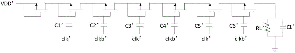
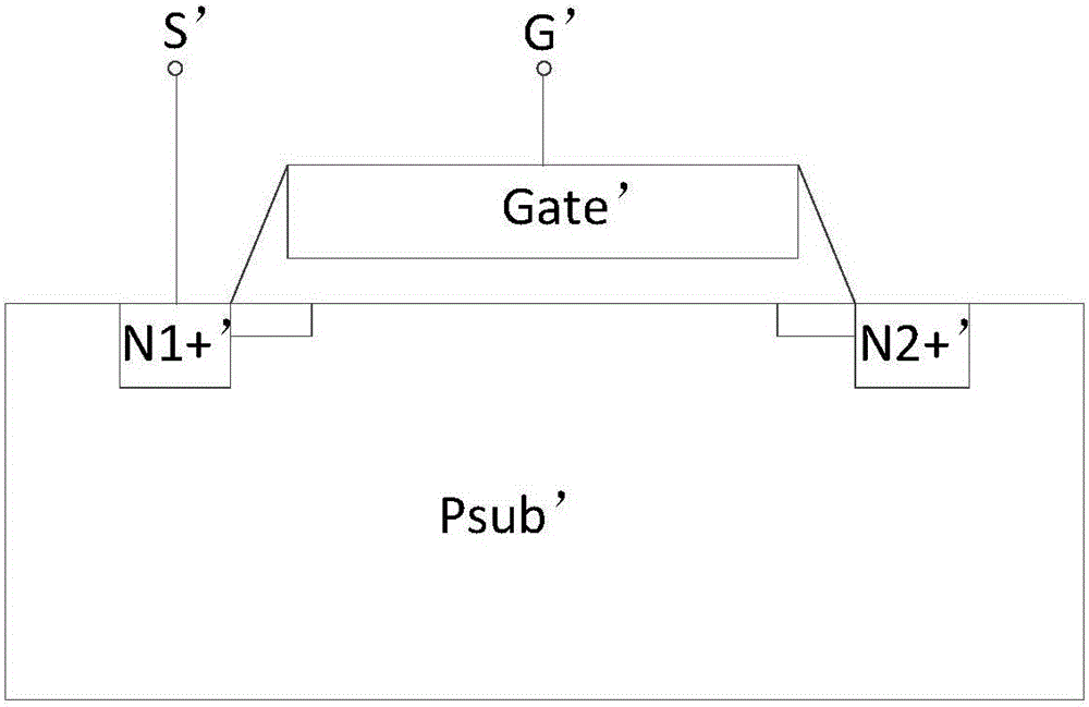
[0021] refer to Figure 4 , shows a schematic cross-sectional structure diagram of a charging capacitor embodiment of the present invention, the charging capacitor is applied to the pump circuit of the memory, wherein the first terminal G of the charging capacitor is the floating gate control electrode FG of a floating gate MOS transistor in the memory The lead-out terminal of the charging capacitor, the second terminal S of the charging capacitor is the common terminal after connecting the P well contact point P+, the source N1+, and the control gate CG in the floating gate MOS tube, and the power supply terminal VDD of the charging capacitor is the N in the floating gate MOS tube. The leading end of the well NW.

[0022] Specif...


PUM


Abstract

The embodiment of the invention provides a charging capacitor and a pump circuit. The charging capacitor is applied to a pump circuit of a memory; the first end of the charging capacitor is a leading-out end of a floating gate control electrode in a floating gate MOS transistor inside the memory; the second end of the charging capacitor is a common end after a P-well contact point in the floating gate MOS transistor, a source electrode and a control gate electrode; and the power supply end of the charging capacitor is a leading-out end of an N well in the floating gate MOS transistor. The charging capacitor in the embodiment of the invention can resist high voltage, the equivalent capacitance per unit area is large, and quick and high-efficiency charging can be realized.

Description

technical field [0001] The invention relates to the technical field of memory, in particular to a charging capacitor and a pump circuit. Background technique [0002] The structure diagram of the traditional pump (charge pump) circuit is as follows: figure 1 As shown, in the pump circuit, the area of ​​the charging capacitor accounts for a relatively large proportion of the total area, that is, figure 1 The area of ​​charging capacitor C1', charging capacitor C2', charging capacitor C3', charging capacitor C4', charging capacitor C5' and charging capacitor C6'. figure 1 Among them, clk' and clkb' are clock signals with the same frequency and opposite phases, the resistor RL' and capacitor CL' are the analog equivalent load circuit of the pump circuit, and VDD' is the power supply of the pump circuit. The signal diagram of clk' and clkb' is as follows figure 2 shown. figure 1 MOS (Metal-Oxide-Semiconductor, Metal-Oxide-Semiconductor Field Effect Transistor) tubes are oft...

Claims


Application Information

Patent Timeline
IPC IPC(8): H02M3/07G11C16/06G11C16/30
CPCG11C16/06G11C16/30H02M3/07
Inventor 胡俊陈晓璐刘铭
Owner HEFEI GEYI INTEGRATED CIRCUIT CO LTD
Why Eureka
Try Eureka