Flexible display apparatus and preparation method therefor, and electronic equipment

A technology for flexible display devices and electronic equipment, which is applied to circuits, electrical components, and electrical solid devices, and can solve problems such as screen faults or layers, and overall uneven display effects

Active Publication Date: 2016-07-27
KUNSHAN NEW FLAT PANEL DISPLAY TECH CENT
View PDF3 Cites 4 Cited by
  • Summary
  • Abstract
  • Description
  • Claims
  • Application Information

AI Technical Summary

Problems solved by technology

[0004] Based on this, it is necessary to provide a flexible display device, a preparation method and an electronic device for the probl

Method used


Image

  • Flexible display apparatus and preparation method therefor, and electronic equipment
  • Flexible display apparatus and preparation method therefor, and electronic equipment
  • Flexible display apparatus and preparation method therefor, and electronic equipment

Examples


preparation example Construction

[0080] As a specific embodiment of the flexible display device manufacturing method of the present invention, it includes the following steps:

[0081] First, through step S100, a PI layer is prepared on the surface of the pretreated substrate. Wherein, the substrate may be a glass substrate. At the same time, the pretreatment of the substrate is specifically cleaning the substrate, which may specifically be cleaned by ultrasonic waves. In addition, when the PI layer is prepared on the surface of the cleaned substrate, it can be prepared by a spin coating process. Then, through step S200, a substrate layer is formed on the surface of the PI layer. Wherein, the preparation of the substrate layer may adopt a CVD (Chemical Vapor Deposition, chemical vapor deposition) process. Furthermore, in step S300, a TFT layer is formed on the surface of the substrate layer. Wherein, the preparation of the TFT layer can adopt CVD process, sputter deposition (Sputter) process, yellow light...

Embodiment 1

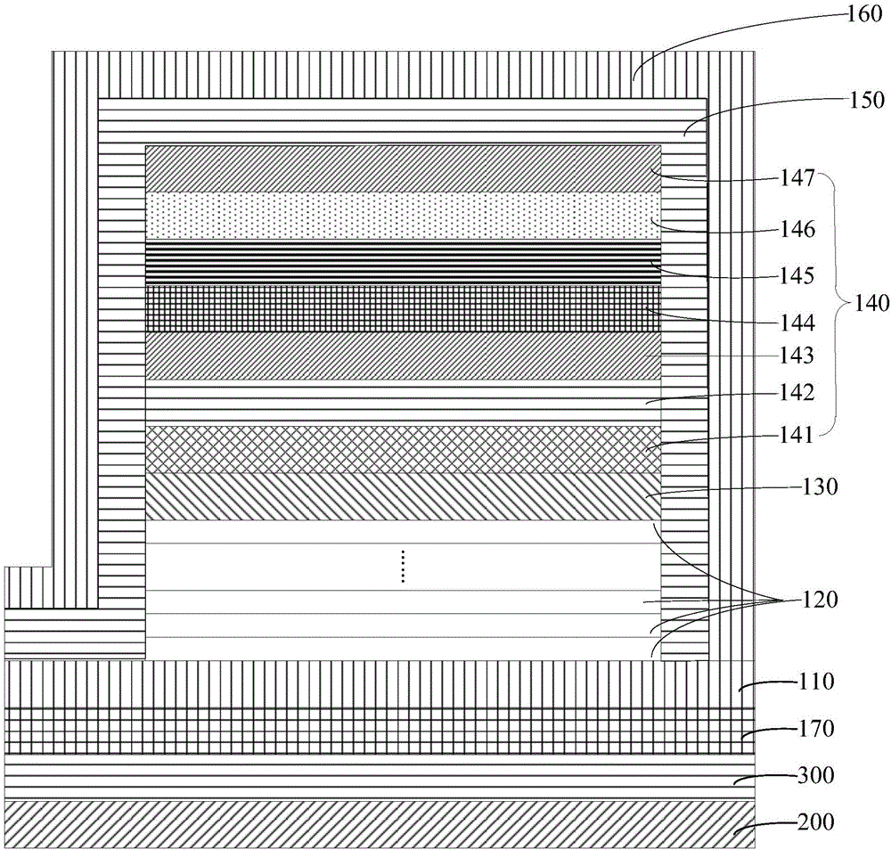
[0089] This embodiment is a preparation process when the protective film is formed on the periphery of the flexible display device through the preparation process. specific:

[0090] First, the glass substrate is cleaned and pretreated. Then, a PI layer was prepared and formed on the glass substrate by a spin-coating process. Then prepare and form a protective film on the PI layer. Furthermore, a BL layer is formed on the protective film by using a CVD process. Further, the TFT structural part and the anode part are sequentially prepared on the surface of the BL layer. Among them, the preparation process of the TFT structure part and the anode part is mainly CVD / Sputter, yellow light, etching, etc.

[0091] Further, the OLED layer is prepared. Specifically, firstly, a hole injection layer (HIL) is prepared on the surface of the anode layer. Wherein, the hole injection layer is made of an organic material, which is made by evaporation, and the hole injection layer is the ...

Embodiment 2

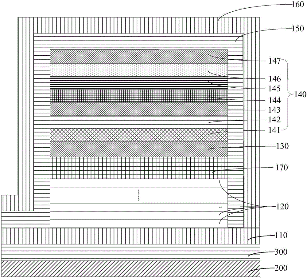
[0094] This embodiment is a preparation process when the protective film is formed on the periphery of the flexible display device by bonding.

[0095] specific:

[0096] First, the glass substrate is cleaned and pretreated. Then, a PI layer was prepared and formed on the glass substrate by a spin-coating process. Furthermore, a BL layer is formed on the protective film by using a CVD process. Further, the TFT structural part and the anode part are sequentially prepared on the surface of the BL layer. Among them, the preparation process of the TFT structure part and the anode part is mainly CVD / Sputter, yellow light, etching, etc.

[0097] Further, the OLED layer is prepared. Specifically, firstly, a hole injection layer (HIL) is prepared on the surface of the anode layer. Wherein, the hole injection layer is made of an organic material, which is made by evaporation, and the hole injection layer is the main carrier of holes. Then, a hole transport layer (HIL) was prepare...


PUM


Abstract

The invention discloses a flexible display apparatus and a preparation method therefor, and electronic equipment. The flexible display apparatus comprises a substrate layer, a TFT layer formed on the substrate layer, a positive electrode layer formed on the TFT layer, an OLED layer formed on the positive electrode layer, a negative electrode layer formed on the OLED layer and the substrate layer which is not covered with the OLED layer, and a packaging layer formed on the negative electrode layer and the substrate layer which is not covered with the negative electrode layer, wherein a packaging space is formed by the packaging layer, the negative electrode layer and the substrate layer; the flexible display apparatus also comprises a protective film which is bent and deformed along with the flexible display apparatus; and the protective film is formed in at least one position as follows: the surface, deviating from the TFT layer, of the substrate layer, the position between the TFT layer and the positive electrode layer, the position between the positive electrode layer and the OLED layer, the position between the OLED layer and the negative electrode layer, the position between the negative electrode layer and the packaging layer, and the surface, deviating from the negative electrode layer, of the packaging layer. The problem of uneven display effect of the screen of the conventional flexible display apparatus is effectively solved.

Description

technical field [0001] The invention relates to the technical field of displays, in particular to a flexible display device, a preparation method and electronic equipment. Background technique [0002] At present, AMOLED (Active-matrix organic light-emitting diode, active-matrix organic light-emitting diode) as a new type of display has high chromaticity, high contrast, wide viewing angle, high brightness, self-illumination, fast response, and flexible display. And other features, has been widely used in electronic devices such as mobile phones and media players. [0003] Among them, the flexible display device realized by AMOLED has the advantages of being able to maintain the unfolded state for easy operation when working, keep the curled state for easy carrying when storing, and can also be hung on the body to present a wearable state, making it widely concerned. However, when the traditional flexible display device is applied to flexible display occasions, since the ben...

Claims


Application Information

Patent Timeline
IPC IPC(8): H01L27/32H01L51/52H01L51/56
CPCH10K59/12H10K50/844H10K71/00
Inventor 丁立薇张婷婷朱晖张小宝
Owner KUNSHAN NEW FLAT PANEL DISPLAY TECH CENT
Why Eureka
Try Eureka