Chemical mechanical grinding method

A technology of chemical machinery and grinding method, which is applied in the direction of grinding devices, grinding machine tools, and parts of grinding machine tools, etc., which can solve problems such as surface scratches, and achieve the effect of avoiding scratches and preventing significant increase

Inactive Publication Date: 2016-08-03
SEMICON MFG INT (SHANGHAI) CORP
View PDF9 Cites 13 Cited by
  • Summary
  • Abstract
  • Description
  • Claims
  • Application Information

AI Technical Summary

Problems solved by technology

[0006] The problem solved by the present invention is the problem of scratches on the surface of the wafer to be polished in the prior art after chemical mechanical polishing

Method used


Image

  • Chemical mechanical grinding method
  • Chemical mechanical grinding method
  • Chemical mechanical grinding method

Examples


Embodiment Construction

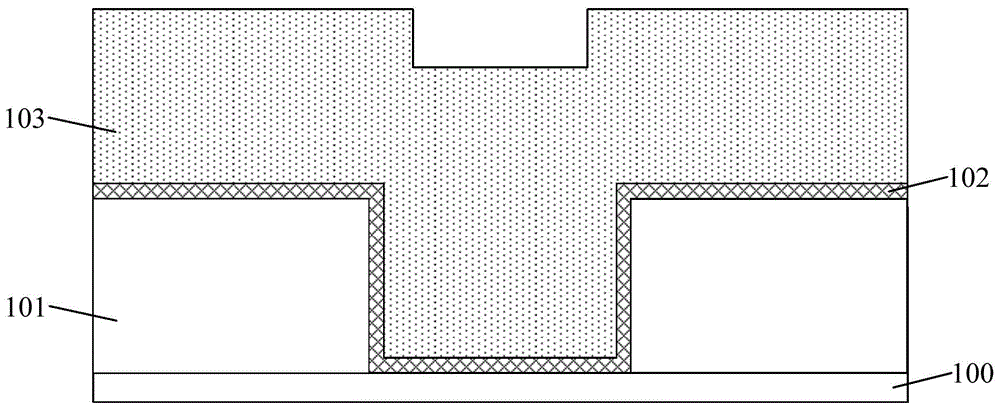
[0034] It can be seen from the background art that in the prior art, after chemical mechanical polishing is performed on the wafer to be polished, there are scratches on the surface of the wafer to be polished, and the scratches lead to a low production yield of the semiconductor structure.

[0035] It has been found through research that common grinding liquids include abrasives, reactants and deionized water, and the abrasives are generally silica or alumina. Microscopic particles (microscopic particles) can be produced in the grinding liquid itself. When the particulate matter is suspended in the grinding liquid, the particles repel or attract each other, so that a charged layer is formed in the grinding liquid, so that the wafer to be ground The surface develops a zeta potential, which is either positive or negative.

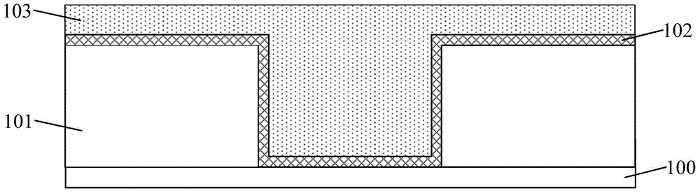
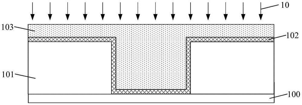
[0036] When the wafer to be ground is ground, at least the following steps are included: step S1, the surface of the wafer to be ground is first ground, and...


PUM


Abstract

The invention discloses a chemical mechanical grinding method which includes the following steps: a wafer to be ground is arranged on a first grinding pad; first grinding is conducted the wafer by first grinding liquid; the first grinding liquid has a first pH value, so the wafer to be ground can be separated from the first grinding pad; first cleaning liquid is sprayed on the surface of the wafer to be ground to conduct first cleaning; the first cleaning liquid has a second pH value; an absolute value of a difference between the first and second Ph values is no more than 1; after the first cleaning, the wafer to be ground is placed on a second grinding pad; second grinding is conducted to the wafer to be ground via second grinding liquid; the second grinding liquid has a third pH value; and an absolute value of a difference between the third pH value and the second pH value is no more than 1. Acid-base conflict can be prevented for the surface of the wafer to be ground, so plenty of microcosmic particles can be prevented from appearing on the surface of the wafer to be ground; and scraps to the surface of the wafer to be ground by the microcosmic particles during the second grinding can be avoided.

Description

technical field [0001] The invention relates to the technology in the field of semiconductor manufacturing, in particular to a chemical mechanical polishing method. Background technique [0002] With the rapid development of ultra-large-scale integrated circuits, the manufacturing process of integrated circuits has become more and more complex and surprising. In order to improve integration and reduce manufacturing costs, the size of semiconductor devices is decreasing day by day, and planar wiring has been difficult to meet the high-density distribution of semiconductor devices. It has become one of the development trends to use multi-layer wiring technology to increase the integration density of semiconductor devices. Among them, chemical mechanical polishing (CMP, Chemical Mechanical Polishing) technology can realize the flattening of the entire wafer, which is an important process in the semiconductor manufacturing process. one of the steps. [0003] The equipment used ...

Claims


Application Information

Patent Timeline
Patent Type & Authority Applications(China)
IPC IPC(8): B24B37/10B24B37/005B24B53/017H01L21/321
Inventor 邓武锋蒋莉黎铭琦赵简杨俊
Owner SEMICON MFG INT (SHANGHAI) CORP
Why Eureka
Try Eureka