Indium bump device structure and preparation method for same

A device structure and bump technology, which is applied in the manufacturing of semiconductor devices, electrical components, and final products, etc., can solve problems affecting device performance and stability, shorten device life, etc., and achieve the effect of high structural strength and high stability.

Inactive Publication Date: 2016-08-03
KUNMING INST OF PHYSICS
View PDF3 Cites 19 Cited by
  • Summary
  • Abstract
  • Description
  • Claims
  • Application Information

AI Technical Summary

Problems solved by technology

[0008] The above two situations will affect the performance a

Method used


Image

  • Indium bump device structure and preparation method for same
  • Indium bump device structure and preparation method for same
  • Indium bump device structure and preparation method for same

Examples


Embodiment Construction

[0041] The present invention will be further described in detail below in conjunction with the examples.

[0042] Those skilled in the art will understand that the following examples are only for illustrating the present invention and should not be considered as limiting the scope of the present invention. If no specific technique or condition is indicated in the examples, it shall be carried out according to the technique or condition described in the literature in this field or according to the product specification. The reagents or instruments used were not indicated by the manufacturer, and they were all conventional products that could be purchased.

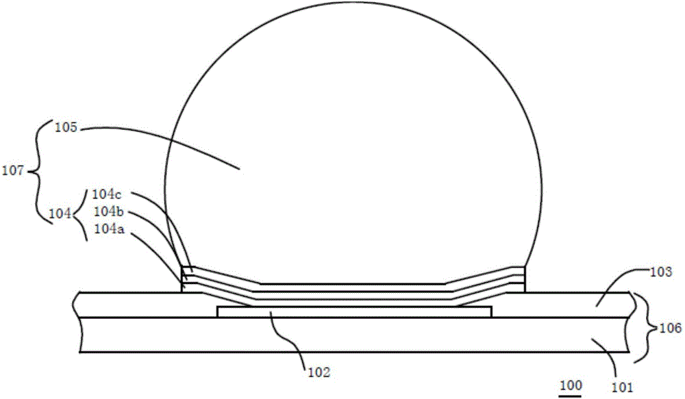
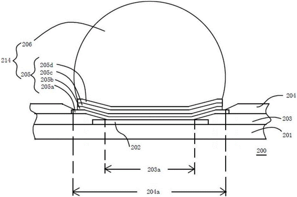
[0043] Those skilled in the art should understand that since the layered structure of the present invention overlaps, the two sides of the first opening 203 a and the second opening 204 a are drawn out and then marked, and the drawn width is also the cross-sectional width.

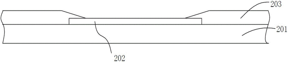
[0044] figure 2 Shown is a cross-sectional stru...


PUM


Abstract

The invention relates to an indium bump device structure and a preparation method for the same and belongs to the technical field of preparation of indium bump devices. The device structure comprises a semiconductor substrate, a welding disk, a first passivation layer, a second passivation layer, a UBM metal layer and an indium bump, wherein the UBM metal layer comprises an adhesion layer, a blocking layer, a buffer layer and a wetting layer; and in the device structure, a part of the first passivation layer is covered by the adhesion layer, and a part of the adhesion layer is covered by the second passivation layer. High structural intensity is provided by the stacking structure, so that the structure composed of the indium bump and the UBM is prevented from being separated along an interface of the adhesion layer and the first passivation layer under effects of thermal stress when the device surfers from thermal shocks. In addition, internal stress changes between the substrate and the UBM during backflow are mitigated by setting of the buffer layer, so that the indium bump is prevented from being separated from the wetting layer under too large internal stress changes. Hence, the device structure provided by the invention has higher stability and a longer service life.

Description

technical field [0001] The invention belongs to the technical field of indium bump device preparation, and in particular relates to an indium bump device structure and a preparation method thereof. Background technique [0002] At present, infrared focal plane detectors have been widely used in military, industry, environment, medicine, etc., and with the advancement of science and technology, people's demand for large area array detectors is increasing. However, with the increase of the number of picture elements, the difficulty of designing and interconnecting the focal plane and the readout circuit is also increasing. Traditional gold wire bonding technology has exposed obvious disadvantages, such as: high interconnection resistance, long circuit, large package size and low interconnection density. Flip-chip interconnection technology can not only overcome the above-mentioned shortcomings, but also has low cost, so it is widely used. [0003] In the infrared detector fl...

Claims


Application Information

Patent Timeline
IPC IPC(8): H01L31/09H01L31/0224H01L31/0352H01L31/18
CPCH01L31/022425H01L31/0352H01L31/09H01L31/18Y02P70/50
Inventor 杨超伟李京辉韩福忠王琼芳封远庆左大凡杨毕春周连军吴圣娟
Owner KUNMING INST OF PHYSICS
Why Eureka
Try Eureka