
Detection method for deep layer impurity element

A technology of impurity elements and detection methods, which is applied in the direction of measuring devices, electrical components, semiconductor/solid-state device testing/measurement, etc., can solve the problems that affect the detection accuracy, blockage of sampling cones, and inability to perform, so as to achieve accurate and reliable detection results Effect

Inactive Publication Date: 2016-08-17
SHANGHAI HUALI MICROELECTRONICS CORP
View PDF4 Cites 4 Cited by
  • Summary
  • Abstract
  • Description
  • Claims
  • Application Information

AI Technical Summary

Problems solved by technology

[0006] The present invention aims at the limitation of the traditional method for detecting impurity elements in deep layers in the prior art, and the sampling cone of the inductively coupled plasma mass spectrometer is likely to cause blockage, thereby affecting the detection accuracy, or the detection depth exceeds the inductively coupled plasma mass spectrometer Defects such as the detection limit of the instrument cannot be detected Provide a detection method for deep impurity elements

Method used


Image

  • Detection method for deep layer impurity element
  • Detection method for deep layer impurity element

Examples


Embodiment Construction

[0022] In order to illustrate the technical content, structural features, achieved goals and effects of the present invention in detail, the following will be described in detail in conjunction with the embodiments and accompanying drawings.

[0023] As we all know, impurity element pollution, especially metal impurity pollution, has a great impact on the performance of semiconductor devices. The level of metal impurity pollution directly determines the white pixel level of CMOS image sensor (CMOS Image Sensor, CIS) products, and ultimately affects the photo effect. Obviously, the monitoring of metal impurity contamination is particularly important in the manufacture of semiconductor devices.

[0024] At present, the industry's monitoring of metal impurity contamination is limited to the use of inductively coupled plasma mass spectrometry (ICP-MS), which has its own inherent defects. For example, the detection of impurity elements in shallow layers is more accurate, but the de...


PUM

PropertyMeasurementUnit
thicknessaaaaaaaaaa

Abstract

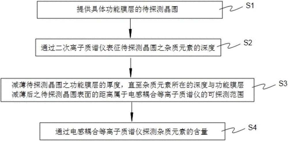
Disclosed is a detection method for a deep layer impurity element. The detection method comprises the steps of step S1, providing a to-be-detected wafer with a function film layer; step S2, representing the depth of the impurity element of the to-be-detected wafer through a secondary ion mass spectrometer; step S3, thinning the functional film layer until the distance from the depth of the impurity element to the surface of the to-be-detected wafer belongs to a detection depth range of an inductive coupling plasma spectrometer; and S4, detecting the content of the impurity element through the inductive coupling plasma spectrometer. According to the detection method, the depth of the impurity element of the to-be-detected wafer is represented by the secondary ion mass spectrometer; then the thickness of the functional film layer is thinned until the distance from the depth of the impurity element to the surface of the to-be-detected wafer after the functional film layer is thinned belongs to the detection depth range of the inductive coupling plasma spectrometer; and finally, the content of the impurity element is detected through the inductive coupling plasma spectrometer. Therefore, a sampling cone is not blocked in the sampling process; and meanwhile, the detection result is accurate and reliable.

Description

technical field [0001] The invention relates to the technical field of semiconductor manufacturing, in particular to a detection method for deep impurity elements. Background technique [0002] As we all know, impurity element pollution, especially metal impurity pollution, has a great impact on the performance of semiconductor devices. The level of metal impurity pollution directly determines the white pixel level of CMOS image sensor (CMOS Image Sensor, CIS) products, and ultimately affects the photo effect. Obviously, the monitoring of metal impurity contamination is particularly important in the manufacture of semiconductor devices. [0003] At present, the industry's monitoring of metal impurity contamination is limited to the use of inductively coupled plasma mass spectrometry (ICP-MS), which has its own inherent defects. For example, the detection of impurity elements in shallow layers is more accurate, but the detection of impurity elements in deep layers cannot be ...

Claims


Application Information

Patent Timeline
Patent Type & Authority Applications(China)
IPC IPC(8): H01L21/66G01N27/62G01N27/626
CPCH01L22/12G01N27/62
Inventor 袁立军赖朝荣苏俊铭
Owner SHANGHAI HUALI MICROELECTRONICS CORP
Learn More