LED (Light Emitting Diode) packaging structure and packaging method thereof

A technology of LED packaging and LED chips, applied in electrical components, circuits, semiconductor devices, etc., can solve the problems of inability to form a flat surface, poor tin-eating ability of pins, design height error, etc., to increase the tin-eating area, The effect of streamlining production processes and improving reliability

Inactive Publication Date: 2016-08-17
WUHU JUFEI PHOTOELECTRIC TECH CO LTD
View PDF5 Cites 5 Cited by
  • Summary
  • Abstract
  • Description
  • Claims
  • Application Information

AI Technical Summary

Problems solved by technology

The CHIP type LED device with this structure only has tin on the back pad. Compared with the "L" type pin, the tinning effect is poor, and it is easy to cause false soldering of the LED device.
[0005] In the second type of LED device, in order to solve the problem that only the pad on the back of the LED device can eat tin, compared with the "L" type pin, the tinning effect is poor, and it is easy to cause the problem of virtual soldering of the LED device, such as image 3 As shown, the patent application number is CN20151049071.1, and the title is the invention patent of LED packaging structure and its packaging method. Although this technical solution can solve the problems of poor soldering ability and high soldering rate of pins
However, this technical solution cannot accurately control the amount of filling, and cannot accurately reserve the height of the tin, and there will be a large error between the height of the vacated through hole and the design height
Also because the filler is a flowable substance, the surface of the filler cannot form a flat surface, which affects the appearance and tinning effect

Method used


Image

  • LED (Light Emitting Diode) packaging structure and packaging method thereof
  • LED (Light Emitting Diode) packaging structure and packaging method thereof
  • LED (Light Emitting Diode) packaging structure and packaging method thereof

Examples


Embodiment Construction

[0034] In order to fully understand the technical content of the present invention, the technical solutions of the present invention will be further introduced and illustrated below in conjunction with specific examples, but not limited thereto.

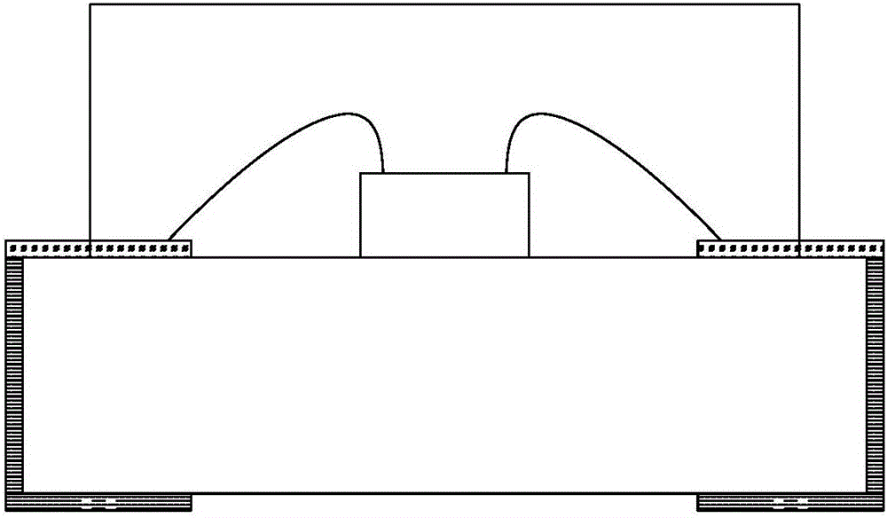
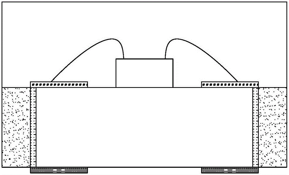
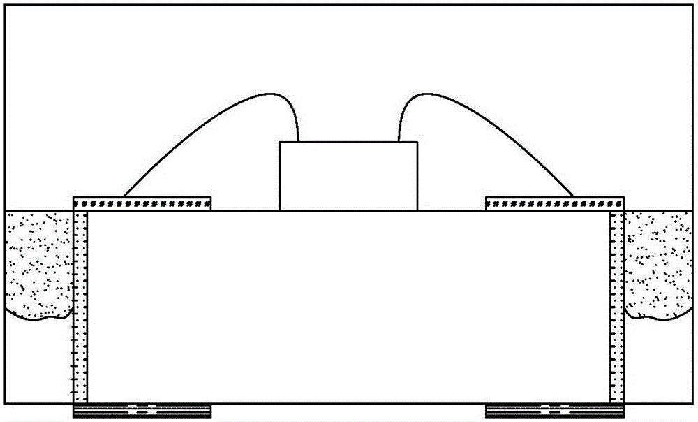
[0035] Such as Figure 4 As shown, an LED packaging structure includes a PCB substrate 1; the upper surface of the PCB substrate 1 is provided with a soldering functional area 2, and the lower surface is fixed with a pin 3; the soldering functional area 2 is electrically connected to the pin 3; The upper surface of the PCB substrate 1 is also provided with an LED chip 4; the LED chip 4 is electrically connected to the solid welding functional area 2 through the bonding wire 5; the upper surface of the PCB substrate 1 is also provided with a colloid 6 for fixing the LED chip 4; 1 includes two layers of plates that are overlapped and fixedly connected together; the lower plate 11 is provided with a first through hole 111, and the thick...


PUM


Abstract

The invention relates to an LED packaging structure and a packaging method thereof; the LED packaging structure includes a PCB substrate with a solid-welding functional area and an LED chip on the upper surface and pins fixed on the lower surface; the solid-welding functional area and the pin electrical Connection; the LED chip is electrically connected to the solid soldering functional area; the PCB substrate includes two layers of overlapping and fixedly connected plates; the lower plate is provided with a first through hole, and the thickness is the same as the reserved tinning height; the first through The inner surface of the hole is provided with a metal layer; the pin is electrically connected to the metal layer; the upper plate is provided with a second through hole; the second through hole is filled with conductive metal; the soldering functional area and the second through hole The conductive metal is electrically connected; the conductive metal in the second through hole is electrically connected with the metal layer on the inner surface of the first through hole. This structure increases the tin eating area during welding and improves the reliability of subsequent welding; since the reserved tin eating position is highly controllable, the production process of the PCB substrate is simplified.

Description

technical field [0001] The invention relates to LED packaging technology, in particular to an LED packaging structure and a packaging method thereof. Background technique [0002] The front pad of the LED device is used to place the chip, and the back pad is used for tinning; there are two connection methods between the front pad and the back pad: [0003] The first LED device, such as figure 1 As shown, the "L"-shaped pin is formed by bending the metal foot, and the front and back electrical connections are formed through the "L"-shaped pin. [0004] The second LED device, such as figure 2 As shown, the PCB substrate is drilled at a specific position, and electroplating and chemical processes are used to form electroplated metal on the hole wall on the through hole, and the front and back electrical connections are formed through the through hole. In order to prevent the LED device packaging glue from overflowing from the front to the back or the solder paste from overf...

Claims


Application Information

Patent Timeline
Patent Type & Authority Applications(China)
IPC IPC(8): H01L33/48H01L33/62
CPCH01L33/486H01L33/62H01L2933/0066
Inventor 甘树威张妮邢其彬童文鹏
Owner WUHU JUFEI PHOTOELECTRIC TECH CO LTD
Why Eureka
Try Eureka