Side-wall-coarsened high-brightness light emitting diode and preparation method thereof

A light-emitting diode, high-brightness technology, used in electrical components, circuits, semiconductor devices, etc., can solve the problems of many production steps, high production costs, complex processes, etc., to improve product reliability, reduce refractive index difference, and improve luminescence. The effect of efficiency

Inactive Publication Date: 2016-08-31
NANCHANG KAIXUN PHOTOELECTRIC CO LTD
View PDF5 Cites 2 Cited by
  • Summary
  • Abstract
  • Description
  • Claims
  • Application Information

AI Technical Summary

Problems solved by technology

At the same time, the surface roughening technology can improve the total reflection at the interface between the AlGaInP chip and the packaging material, and the brightness will be higher. However, due to the many manufacturing steps and the very complicated process, the manufacturing cost is high and the yield is low.

Method used


Image

  • Side-wall-coarsened high-brightness light emitting diode and preparation method thereof

Examples


Embodiment Construction

[0027] The present invention will be described in further detail below in conjunction with the embodiments and with reference to the accompanying drawings.

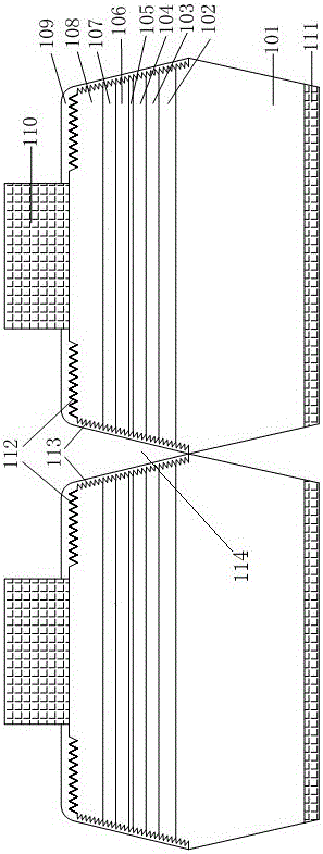
[0028] A high-brightness light-emitting diode with roughened side walls, including a gallium arsenide permanent substrate 101 , on a GaAs permanent substrate 101 set above in turn with N-GaAs The buffer layer 102 、 AlAs / AlGaAs reflective layer 103 、 N-AlGaInP lower limiting layer 104 、 AlGaInP active layer 105 、 P-AlGaInP upper limit layer 106 、 P-GaInP The buffer layer 107 and P-GaP Coarsening layer 108 , P-GaP Coarsening layer 108 Include P-GaP Front Coarsening Layer 112 and P-GaP roughened sidewall 113 two parts, in P-GaP Front Coarsening Layer 112 set the first electrode on 110 , P-GaP roughened sidewall 113 presented V groove structure, window layer 109 for SiN Optical Thin Films, Permanent Substrates on Gallium Arsenide 101 A s...


PUM


Abstract

The invention discloses a side-wall-coarsened high-brightness light emitting diode and a preparation method thereof. The side-wall-coarsened high-brightness light emitting diode comprises a gallium arsenide permanent substrate. A buffer layer, a light emitting layer, a window layer and a first electrode are successively arranged on the upper surface of the gallium arsenide permanent substrate. The buffer layer is made of n type gallium arsenide. The light emitting layer comprises an AlAS / AlGaAs reflection layer, an N-AlGaInP lower restriction layer, an AlGaInP active layer, a P-AlGaInP upper restriction layer, a P-GaInP buffer layer and a P-GaP coarsening layer. The P-GaP coarsening layer comprises a P-GaP positive coarsening layer and a P-GaP side wall coarsening layer. The first electrode is arranged on the P-GaP positive coarsening layer. The P-GaP side wall coarsening layer is of a V-shaped groove structure. The window layer is made of a SiN optical film. A second electrode is arranged on the lower surface of the gallium arsenide permanent substrate. The coarsened surface is covered by a passive film SiN, the refractive index difference between the light emitting layer and the packaging material is reduced, the emitting of light is facilitated, the abnormal electricity leakage of a light emitting area is prevented, and the reliability of the product is improved.

Description

technical field [0001] The invention relates to the field of semiconductor light-emitting diodes, in particular to a high-brightness light-emitting diode with roughened side walls and a preparation method thereof. Background technique [0002] Quaternary AlGaInP is a semiconductor material with direct wide bandgap, which has been widely used in the preparation of various optoelectronic devices. Since the luminescence band of AlGaInP material can cover the red to yellow-green band of visible light, the visible light-emitting diodes made from it have attracted extensive attention. [0003] The surface layer of the traditional vertical AlGaInP light-emitting diode is the GaP window layer. Due to the large refractive index difference between GaP and the packaging material, most of the light is totally reflected when it exits the GaP window layer, resulting in low light extraction efficiency. Some people use surface roughening technology to change the light angle, but the effect...

Claims


Application Information

Patent Timeline
Patent Type & Authority Applications(China)
IPC IPC(8): H01L33/22H01L33/00
CPCH01L33/22H01L33/0062
Inventor 张银桥潘彬
Owner NANCHANG KAIXUN PHOTOELECTRIC CO LTD
Why Eureka
Try Eureka