A device and system for suppressing potential-induced decay
A potential-induced attenuation, photovoltaic system technology, applied in circuit devices, output power conversion devices, circuits, etc., can solve problems such as high cost and affect the reliability of photovoltaic systems, and achieve low cost, low power consumption, and small capacity. Effect
- Summary
- Abstract
- Description
- Claims
- Application Information
AI Technical Summary
Problems solved by technology
Method used
Image
Examples
Embodiment 1
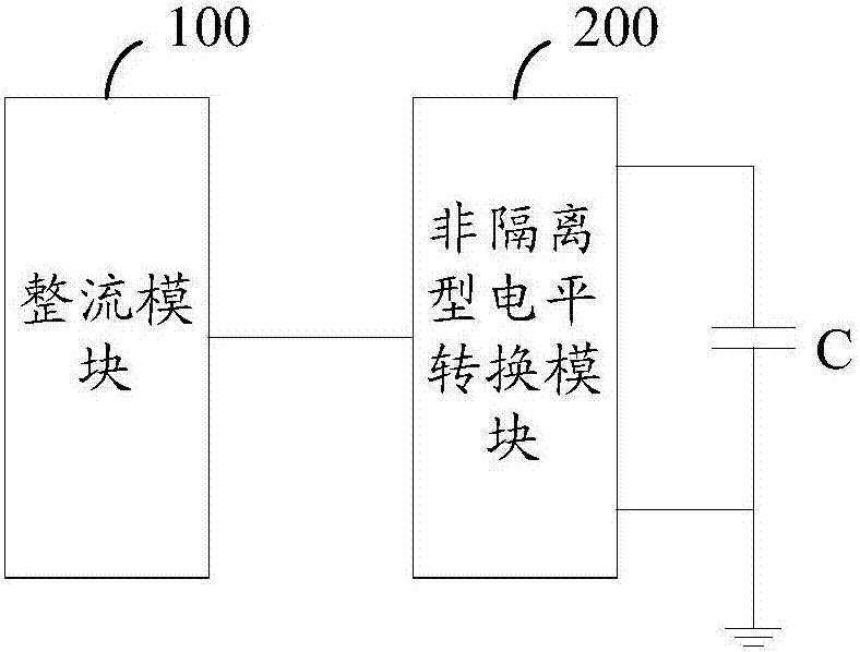
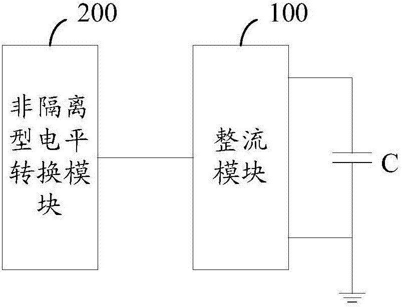
[0057] See Figure 1a with Figure 1b This figure is a schematic diagram of the first embodiment of the device for suppressing the attenuation induced by electric potential provided by the present invention.
[0058] The device for suppressing the attenuation induced by electric potential provided by this embodiment is connected between the AC output end of the converter in the photovoltaic system and the grid-connected power frequency transformer; the device includes: a rectifier module 100 and a non-isolated level conversion module 200 and at least one capacitor C;
[0059] Such as Figure 1a As shown, the input end of the rectification module 100 is connected to the output end of the converter; the rectification module 100 is used to rectify the alternating current output by the converter into direct current; the non-isolated level conversion The module 200 is used for level conversion of the direct current output by the rectification module; the level conversion is a boost conver...
Embodiment 2
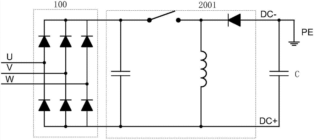
[0067] See Figure 2a with Figure 2b , This figure is a schematic diagram of Embodiment 2 of the device provided by the present invention.
[0068] In this embodiment, when the input terminal of the rectifier module 100 is connected to the output terminal of the converter: the non-isolated level conversion module is specifically any one of the following: Boost circuit, Buck-boost circuit , Cuk circuit, Sepic circuit and Zeta circuit.
[0069] It should be noted that the rectifier module 100 in this embodiment is an uncontrolled rectifier bridge as an example for introduction. Such as Figure 2a As shown, the uncontrolled rectifier bridge is a three-phase full bridge circuit.
[0070] In this embodiment, the non-isolated level conversion module is the Buck-boost circuit 2001 for introduction; the output terminal of the Buck-boost circuit 2001 is connected in parallel with the capacitor C;
[0071] When the positive pole of the capacitor C is grounded, the voltage of the photovoltaic ...
Embodiment 3
[0079] See Figure 4a with Figure 4b , This figure is a schematic diagram of Embodiment 3 of the device provided by the present invention.
[0080] In the device provided in this embodiment, when the input terminal of the rectifier module 100 is connected to the output terminal of the converter: the non-isolated level conversion module is the Boost circuit 2002; the output terminal of the Boost circuit 2002 is connected in parallel The capacitance C;
[0081] Such as Figure 4a As shown, when the negative electrode of the capacitor C is grounded, the output voltage of the non-isolated level conversion module is controlled to make the voltage of the photovoltaic system to the ground positive.
[0082] Such as Figure 4b As shown, when the positive pole of the capacitor C is grounded, the voltage of the photovoltaic system to the ground is negative by controlling the output voltage of the non-isolated level conversion module.
[0083] Combine below Figure 5a Description Figure 4a The...
PUM
 Abstract
Description
Claims
Application Information


