Wafer and solar cell photoinduced carrier radiation phase lock imaging detection method and system

A technology of solar cells and photo-induced carriers, which is applied in the monitoring of photovoltaic systems, photovoltaic power generation, photovoltaic modules, etc., can solve the problems of complex process, pollution, low signal-to-noise ratio, etc., to achieve high detection efficiency and improve signal-to-noise ratio. The effect of larger than the detection area

Inactive Publication Date: 2016-08-31
HARBIN INST OF TECH
View PDF2 Cites 12 Cited by
  • Summary
  • Abstract
  • Description
  • Claims
  • Application Information

AI Technical Summary

Problems solved by technology

[0002] Since semiconductors and their products (electronic components, solar cells, etc.) are used as functional materials and important renewable energy conversion devices, they are widely used in many fields, especially solar cells have received extensive attention under the background of today's energy scarcity, and their demand has increased year by year , but due to the complex process in the production and preparation process, the wafer and its finished products are prone to cause various defects (such as uneven growth, dead knots, mechanical scratches, etc.) Seriously affect its subsequent use performance, increase product production costs, and reduce production efficiency
[0003] At present, the non-destructive testing technology of solar cell imaging is mainly electroluminescence method and photoluminescence detection technology. The electroluminescence method cannot detect samples without pn junctions such as wafers, and this method needs to be carried out in a dark room, and the signal-to-noise ratio Low; photoluminescence detection technology is seriously affected by background noise, so the signal-to-noise ratio is relatively low

Method used


Image

  • Wafer and solar cell photoinduced carrier radiation phase lock imaging detection method and system
  • Wafer and solar cell photoinduced carrier radiation phase lock imaging detection method and system
  • Wafer and solar cell photoinduced carrier radiation phase lock imaging detection method and system

Examples


Embodiment Construction

[0023] The technical solution of the present invention will be further described below in conjunction with the accompanying drawings, but it is not limited thereto. Any modification or equivalent replacement of the technical solution of the present invention without departing from the spirit and scope of the technical solution of the present invention should be covered by the present invention. within the scope of protection.

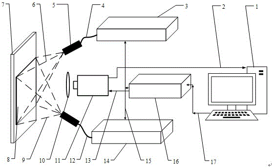
[0024] Such as figure 1 As shown, the carrier radiation lock-in imaging detection system of wafers and solar cells according to the present invention consists of a computer 1, a first signal transmission line 15, a second signal transmission line 17, a third signal transmission line 13, a data transmission line 2, a second signal transmission line A laser 3, a second laser 14, a first optical fiber 4, a second optical fiber 12, a beam shaping device 5, a first laser beam 6, a second laser beam 9, a three-dimensional moving stage 7, a sample to be tested...


PUM


Abstract

The invention discloses a wafer and solar cell photoinduced carrier radiation phase lock imaging detection method and system. The system comprises a near infrared camera, a signal acquisition card, a computer, a three dimensional mobile platform, a long pass filter plate, a first laser device and a second laser device, wherein a sample piece being detected is fixed on the three dimension mobile platform, the three dimension mobile platform is adjusted so as to make the sample piece being detected be clearly visible in a visual field of the near infrared camera, the computer controls the laser devices to subject the sample piece being detected to optical excitation operation by controlling signal acquisition card, the near infrared camera is controlled to be synchronously triggered to collect image sequences, the image sequences collected by the near infrared camera are sent to the computer and then subjected to phase lock processing operation, and therefore high signal to noise ratio carrier radiation signal imaging can be realized. According to the wafer and solar cell photoinduced carrier radiation phase lock imaging detection method and system, the sample piece is excited by laser light in a surface excitation manner, large area can be detected and high detection efficiency is realized, a phase lock algorithm is adopted, good detection results can be obtained in natural light background without darkroom environment, and convenience of detection is realized.

Description

technical field [0001] The invention relates to a photocarrier radiation phase-locked imaging detection method and system for wafers and solar cells, which is suitable for wafer manufacturing in the fields of satellites, microelectronics, semiconductors, photovoltaics, solar cell production, and component current carrying Sub-testing and evaluation. Background technique [0002] Since semiconductors and their products (electronic components, solar cells, etc.) are used as functional materials and important renewable energy conversion devices, they are widely used in many fields, especially solar cells have received extensive attention under the background of today's energy scarcity, and their demand has increased year by year , but due to the complex process in the production and preparation process, the wafer and its finished products are prone to cause various defects (such as uneven growth, dead knots, mechanical scratches, etc.) Seriously affect its subsequent use perfo...

Claims


Application Information

Patent Timeline
Patent Type & Authority Applications(China)
IPC IPC(8): H02S50/15
CPCH02S50/15Y02E10/50
Inventor 刘俊岩宋鹏袁会敏王扬
Owner HARBIN INST OF TECH
Why Eureka
Try Eureka