
An insulating substrate structure and a power module using the substrate

A technology for insulating substrates and power modules, applied in electrical components, electrical solid devices, circuits, etc., can solve the problems of power module reliability, chip overcurrent burnout, large chip loss, etc., so as to reduce the risk of burnout and reduce input resistance, the effect of improving reliability

Active Publication Date: 2018-07-20
YANGZHOU GUOYANG ELECTRONICS CO LTD
View PDF11 Cites 0 Cited by
  • Summary
  • Abstract
  • Description
  • Claims
  • Application Information

AI Technical Summary

Problems solved by technology

[0003] The power level of the current power module is constantly increasing. Although the current and voltage levels of the power device are constantly increasing, a single power device still cannot meet the needs of high-power converters, so the parallel connection of the internal devices of the power module has become an inevitable choice. The current sharing problem of multiple devices connected in parallel is also highlighted
All the half-bridge structures of existing power modules are connected to two DC input terminals together, and because of the different layout of power devices inside the power module, the parasitic parameters of multiple parallel devices are often inconsistent
When the power module is working, different parasitic parameters will cause inconsistencies in the current passing through the parallel devices. The chip with a large current may fail due to over-current burnout. , the reliability of the power module will also be affected in the long run

Method used


Image

  • An insulating substrate structure and a power module using the substrate
  • An insulating substrate structure and a power module using the substrate
  • An insulating substrate structure and a power module using the substrate

Examples


Embodiment 1

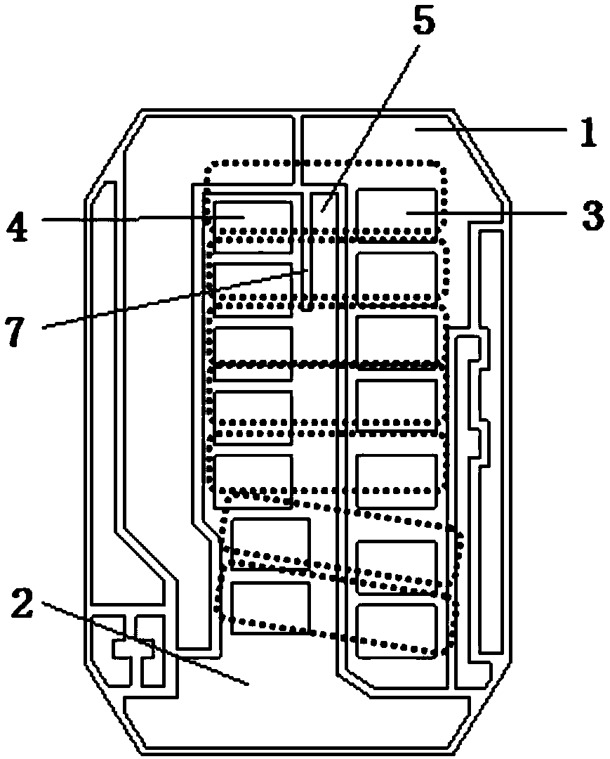
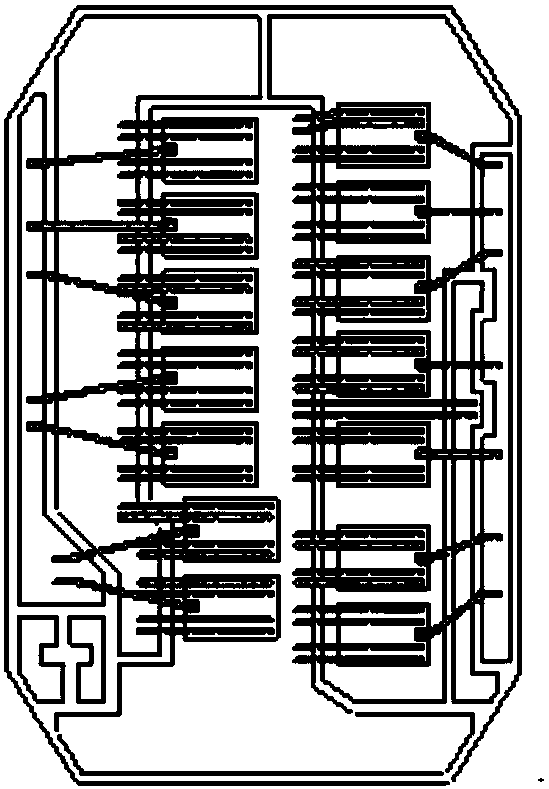
[0028] An insulating substrate structure, and a power module using the structure, the insulating substrate structure is as follows figure 1 As shown, it includes a ceramic insulating layer and a metal layer formed on the ceramic insulating layer. The material of the metal layer is copper or aluminum, and the surface is plated with nickel and gold or nickel and silver. The metal layer is printed by thick film printing technology or brazing technology. Realized, the thickness is 0.1mm-1mm.

[0029] The metal layer includes an upper bridge arm metal layer 1 and a lower bridge arm metal layer 2, the upper bridge arm chip unit 3 is sintered or welded on the upper bridge arm metal layer 1, and the lower bridge arm chip is sintered or welded on the lower bridge arm metal layer 2 Unit 4, the lower bridge arm metal layer 2 includes the wiring area 5, the upper bridge arm chip unit 3 is connected to the wiring area 5 through the bonding wire 6, the bonding wire 6 referred to below is th...

Embodiment 2

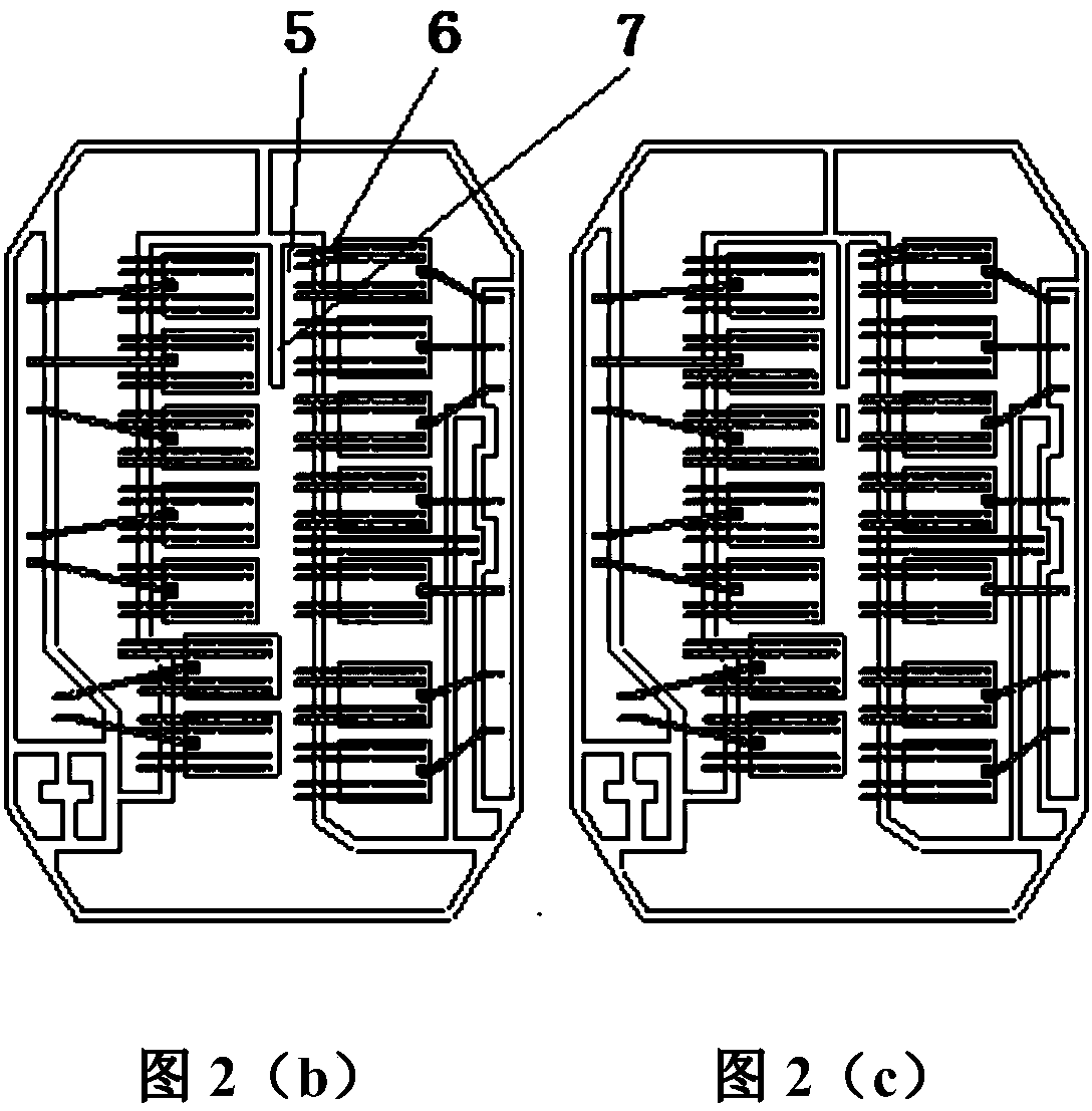
[0039] This embodiment also provides an insulating substrate structure and a power module using the substrate. Its structure is roughly the same as that provided in Embodiment 1. The difference between the two is that the power module in this embodiment adopts the The structure of length balance groove 7 shown in.

Embodiment 3

[0041] This embodiment also provides an insulating substrate structure and a power module using the substrate, such as Image 6 As shown, its structure is roughly the same as that provided in Embodiment 1. The difference between the two is that all the half-bridge structures in this embodiment are connected to two DC input terminals 8. The electrical structure topology diagram is as follows Figure 7 shown.


PUM


Abstract

The invention discloses an insulating substrate structure and a power module using the substrate. The insulating substrate includes a ceramic insulating layer and a metal layer formed on the ceramic insulating layer. The metal layer includes an upper bridge arm metal layer and a lower bridge arm metal layer. The upper bridge arm metal layer is provided with the upper bridge arm chip unit, the lower bridge arm metal layer is provided with the lower bridge arm chip unit, the lower bridge arm metal layer includes the wiring area, and the upper bridge arm chip unit and the wiring area are bonded The lower bridge arm metal layer is provided with an insulating equalization slot between the wiring area and the lower bridge arm chip unit. The invention can protect the power devices close to the DC input terminals, reduce the risk of device burnout due to overload, and balance the parasitic parameters of the parallel devices, especially the parasitic inductance and loop resistance, so as to achieve the effect of current sharing and avoid the burnt due to overcurrent, which improves the reliability of the power module.

Description

technical field [0001] The invention relates to a power semiconductor module, in particular to an insulating substrate structure and a power module using the substrate. Background technique [0002] The global energy crisis and the threat of climate warming make people pay more and more attention to energy conservation, emission reduction and low-carbon development while pursuing economic development. With the establishment and promotion of green environmental protection in the world, the development and application prospects of power semiconductors are broader. [0003] The power level of the current power module is constantly increasing. Although the current and voltage levels of the power device are constantly increasing, a single power device still cannot meet the needs of high-power converters, so the parallel connection of the internal devices of the power module has become an inevitable choice. The current sharing problem of multiple devices connected in parallel is ...

Claims


Application Information

Patent Timeline
Patent Type & Authority Patents(China)
IPC IPC(8): H01L23/15H01L23/498
CPCH01L23/498H01L23/15H01L2224/0603H01L2224/49111H01L2224/49175H01L2924/19107
Inventor 徐文辉滕鹤松方赏华刘凯
Owner YANGZHOU GUOYANG ELECTRONICS CO LTD
Learn More