An internal gate type MOS

A gate type, epitaxial layer technology, applied in semiconductor devices, electrical components, circuits, etc., can solve the problems of large cell size, complex manufacturing process, large chip area, etc. , The effect of reducing the gate-drain capacitance Cgd and reducing Rdson

Inactive Publication Date: 2018-10-26
UNIV OF ELECTRONICS SCI & TECH OF CHINA
View PDF5 Cites 0 Cited by
  • Summary
  • Abstract
  • Description
  • Claims
  • Application Information

AI Technical Summary

Problems solved by technology

However, the NexFET structural cell size is relatively large, the chip area is relatively large, and the manufacturing process is complicated and the cost is high.

Method used


Image

  • An internal gate type MOS
  • An internal gate type MOS
  • An internal gate type MOS

Examples


Embodiment Construction

[0026] Describe technical scheme of the present invention in detail below in conjunction with accompanying drawing

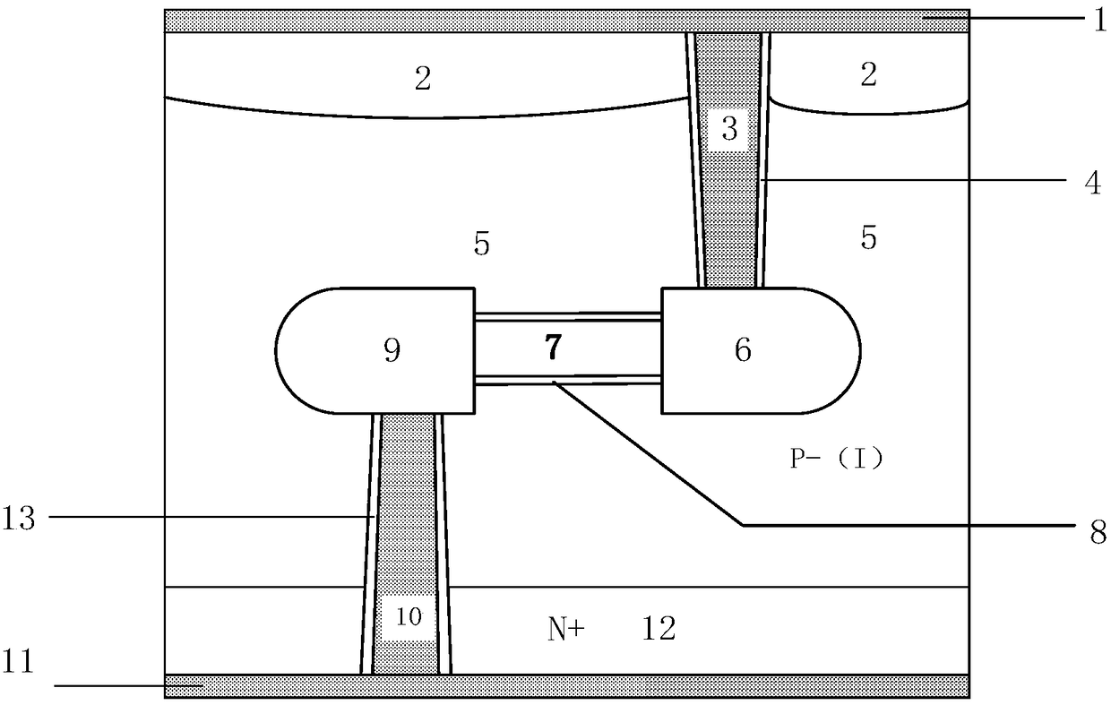
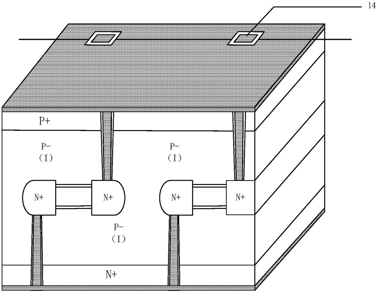
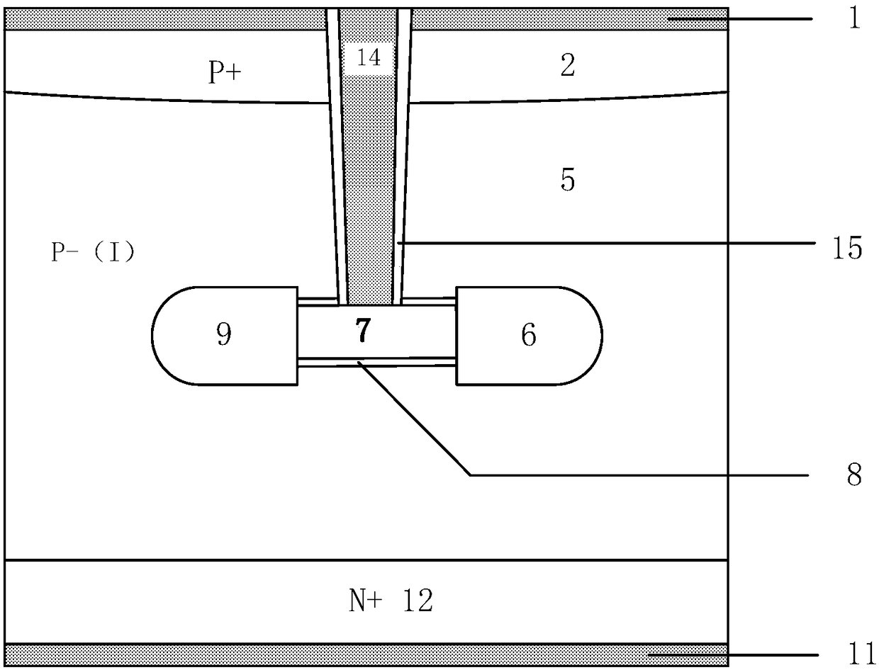
[0027] Such as figure 1 As shown, an internal gate MOS of the present invention includes a drain electrode 11, an N-type heavily doped single crystal silicon substrate 12, a low-doped P-type epitaxial layer 5, a highly doped P+ source region 2 and source metal electrode 1; the doped P-type epitaxial layer 5 has a strip-shaped source region 6 and a strip-shaped drain region 9, and the strip-shaped source region 6 and strip-shaped drain region 9 are located on the same horizontal plane , and the strip-shaped source region 6 and the strip-shaped drain region 9 are connected by a polysilicon gate 7, and the polysilicon gate 7 is isolated from the low-doped P-type epitaxial layer 5 by a gate oxide layer 8; the strip-shaped source region 6 is connected by The first deep groove metal 3 that runs through the highly doped P+ source region 2 is connected to the source me...


PUM


Abstract

The invention belongs to the technical field of power semiconductors, in particular to an internal gate type MOS. The gate and channel of traditional power MOS devices are located on or near the surface of the device, and the source region is usually located on the surface of the device. This invention defines a new channel conduction method, which combines the gate, source region, and drain region It is completely placed in the device body, and the external electrode is connected through the groove gate metal, which greatly reduces the gate-drain capacitance Cgd and gate-source capacitance Cgs of the device. Since the conduction current directly passes through the groove gate metal during forward conduction, the conduction of the structure The resistance is lower than traditional MOS. In reverse withstand voltage, the withstand voltage mechanism of the device is similar to that of a PIN diode, and the low-doped epitaxial layer can withstand higher withstand voltage.

Description

technical field [0001] The invention belongs to the technical field of power semiconductors, in particular to an internal gate type MOS. Background technique [0002] Traditional power VDMOS devices can generally be divided into planar gate VDMOS and trench gate VDMOS devices. The source region and the drain region of these two types of MOS devices are located on the front or back of the device structure. When the device is in the switching state, the gate-drain capacitance C gd , Gate-to-source capacitance C gs It will change due to the change of the applied voltage, so the oscillation of the drain voltage will cause the change of the induced gate potential, which will affect the switching performance of the device under high-frequency working conditions. [0003] At present, many new structures in the world have improved the capacitance of planar gate MOS and trench gate MOS. For example, the NexFET launched by TI in 2010 combines the advantages of lateral device LDMOS a...

Claims


Application Information

Patent Timeline
Patent Type & Authority Patents(China)
IPC IPC(8): H01L29/78H01L29/423H01L29/08H01L29/06
CPCH01L29/0619H01L29/0847H01L29/42356H01L29/78
Inventor 李泽宏陈哲曹晓峰李爽陈文梅任敏
Owner UNIV OF ELECTRONICS SCI & TECH OF CHINA
Why Eureka
Try Eureka