Trench MOSFET (Metal-Oxide-Semiconductor Field-Effect Transistor) and manufacturing method thereof

A manufacturing method and groove-type technology, applied in semiconductor/solid-state device manufacturing, electrical components, electrical solid-state devices, etc., can solve the problems of unit cell spacing limitation and inability to further shrink, so as to avoid stress, facilitate filling, and prevent hollow effect

Active Publication Date: 2011-06-08
WILL SEMICON (SHANGHAI) CO LTD
View PDF3 Cites 24 Cited by
  • Summary
  • Abstract
  • Description
  • Claims
  • Application Information

AI Technical Summary

Problems solved by technology

[0010] The purpose of the present invention is to provide a trench MOSFET to solve the problem that the unit cell spacing of the existing trench MOSFET is limited by the photolithography resolution and cannot be further reduced
[0011] Another object of the present invention is to provide a method for manufacturing a trench MOSFET, so as to solve the problem that the unit cell pitch of the existing trench MOSFET is limited by the photolithography resolution and cannot be further reduced

Method used


Image

  • Trench MOSFET (Metal-Oxide-Semiconductor Field-Effect Transistor) and manufacturing method thereof
  • Trench MOSFET (Metal-Oxide-Semiconductor Field-Effect Transistor) and manufacturing method thereof
  • Trench MOSFET (Metal-Oxide-Semiconductor Field-Effect Transistor) and manufacturing method thereof

Examples


Embodiment Construction
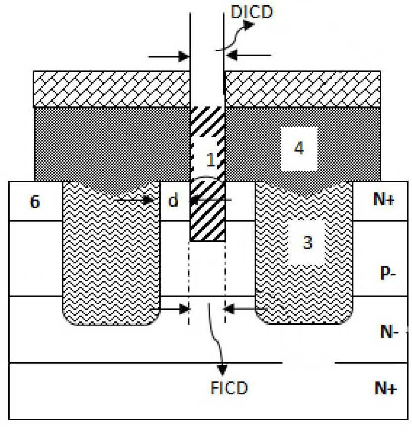
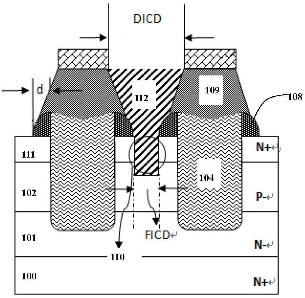
[0052] The main idea of ​​the present invention is to set the source contact hole of the trench MOSFET into a shape with a large upper opening and a small lower opening, so that a small-sized source contact hole can be prepared by using a photolithography process with a larger line width, and can The pitch of the unit cell is further reduced, and the drain-source on-state resistance of the trench MOSFET is reduced.

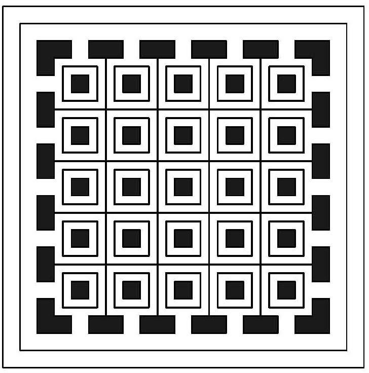
[0053] See figure 2 , which is an overall schematic diagram of the trench MOSFET of the present invention. The trench MOSFET is composed of a large number of unit cells 21 , each square structure in the figure is called a unit cell, and the distance between each unit cell is the distance between adjacent gates. The resistance of the channel under the gate of the unit cell is called the channel resistance, and the channel resistance is the most important parameter of the drain-source on-state resistance. When the drain-source of the MOSFET is turned on, the curr...


PUM


Abstract

The invention provides a trench MOSFET (Metal-Oxide-Semiconductor Field-Effect Transistor) and a manufacturing method thereof. The manufacturing method of the trench MOSFET comprises the following steps of: (1) preparing a heavily doped substrate; (2) forming a lightly doped epitaxial layer on the heavily doped substrate; (3) forming a lightly doped trap region on the lightly doped epitaxial layer; (4) forming a plurality of grid trenches penetrating through the lightly doped trap region and being in contact with the lightly doped epitaxial layer; (5) forming a heavily doped source region at the upper part of the lightly doped trap region and among the grid trenches; (6) forming a side wall on both sides of each grid trench; and (7) forming source electrode contact holes by self alignment of the side walls, wherein the top opening of each contact hole is greater than the bottom opening. The invention can further improve the density of unit cells of MOSFET, provides convenience for etching source electrode contact holes, and is favorable for metal filling of the source electrode contact holes.

Description

technical field [0001] The invention relates to the field of power semiconductor devices, in particular to a high-density cell trench MOSFET and a manufacturing method thereof. Background technique [0002] MOSFET (Power Metal Oxide Semiconductor Field-effect Transistor, field-effect transistor) is widely used in 4C due to its advantages of fast switching speed, good frequency performance, high input impedance, low driving power, good temperature characteristics, and no secondary breakdown problem. (ie Communication, Computer, Consumer, Car: communication, computer, consumer electronics, automobile) and other fields. [0003] The finished trench power MOSFET device is composed of a large number of MOSFET units inside. The MOSFET of each unit is called a unit cell, and the pitch (patch) between the unit cells will directly affect the importance of the power MOSFET. Electrical parameters Drain-source on-state resistance Rdson. The drain-source on-state resistance Rdson is th...

Claims


Application Information

Patent Timeline
Patent Type & Authority Applications(China)
IPC IPC(8): H01L21/768H01L23/52H01L29/78
CPCH01L2924/0002
Inventor 顾建平纪刚倪凯彬钟添宾
Owner WILL SEMICON (SHANGHAI) CO LTD
Why Eureka
Try Eureka