
Semiconductor device

A semiconductor and conductive technology, applied in the direction of semiconductor devices, diodes, electrical components, etc., can solve the problems of high aspect ratio and poor coverage of electrode terminal steps

Inactive Publication Date: 2016-10-05
KK TOSHIBA
View PDF1 Cites 0 Cited by
  • Summary
  • Abstract
  • Description
  • Claims
  • Application Information

AI Technical Summary

Problems solved by technology

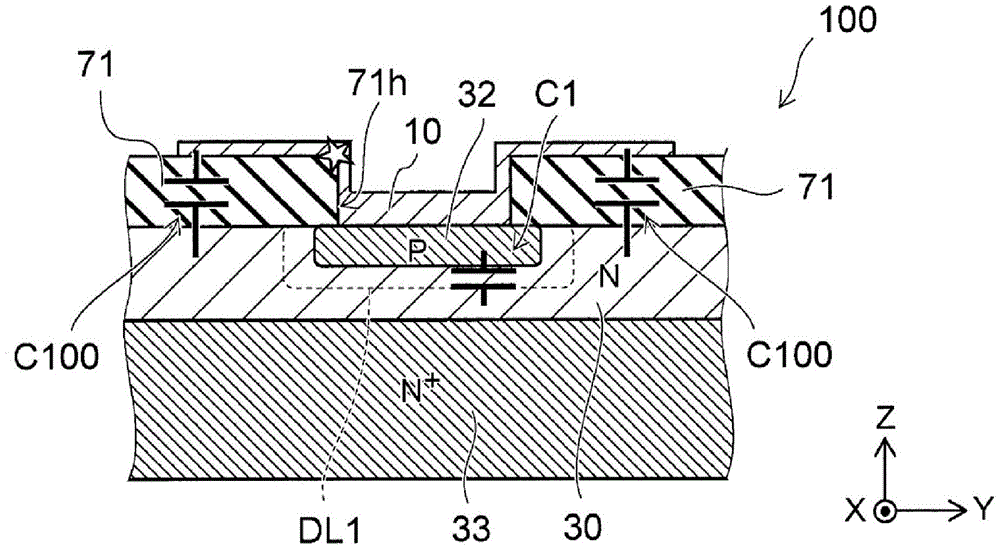
However, if the thickness of the interlayer insulating film is increased, the aspect ratio of the opening of the interlayer insulating film will also increase, and the step coverage of the electrode terminals formed in the opening will deteriorate.

Method used


Image

  • Semiconductor device
  • Semiconductor device
  • Semiconductor device

Examples


no. 1 approach

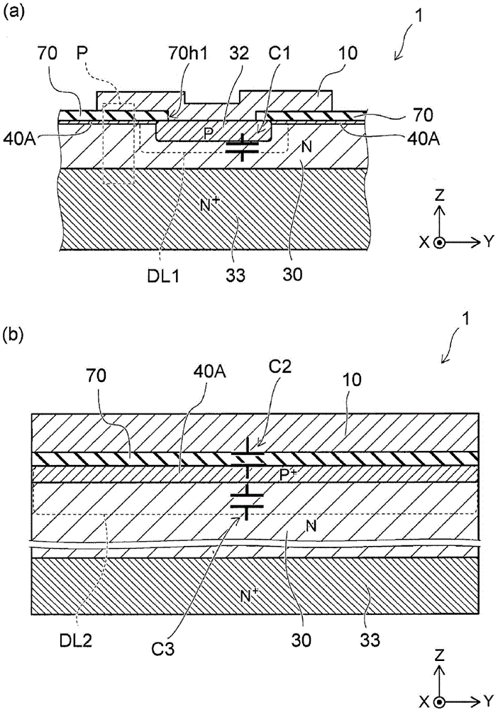
[0016] figure 1 (a) is a schematic sectional view showing a main part of the semiconductor device of the first embodiment, figure 1 (b) is figure 1 An enlarged view of the area enclosed by the dotted line P in (a).

[0017] The semiconductor device 1 according to the first embodiment is an LGA (Land Grid Array) type semiconductor chip including electrode pads (hereinafter, wiring layer 10 ) having a relatively wide area on the surface side.

[0018] The semiconductor device 1 includes an N-type first semiconductor region (hereinafter, for example, the semiconductor region 30 ), a P-type second semiconductor region (hereinafter, for example, the semiconductor region 32 ), a P-type semiconductor region, and a P-type semiconductor region. + type third semiconductor region (hereinafter, eg, semiconductor region 40A), the insulating layer 70 having the first opening (hereinafter, eg, opening 70h1 ), and the wiring layer 10 .

[0019] The semiconductor region 32 is selectively pr...

no. 2 approach

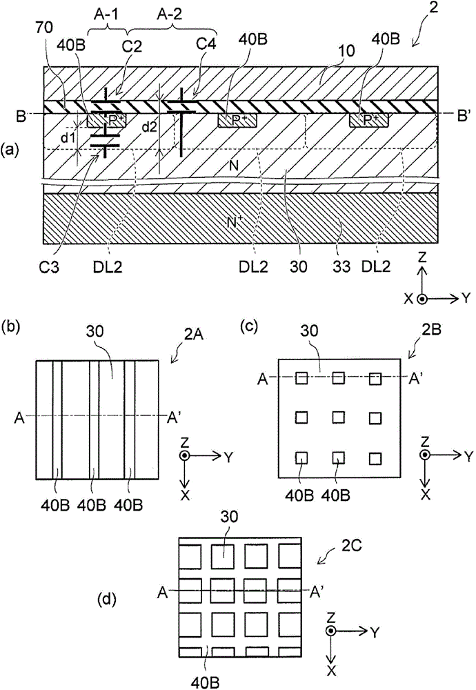
[0036] image 3 (a) shows the main part of the semiconductor device of the second embodiment, and is image 3 (b), (c), (d) schematic cross-sectional view of the line A-A', image 3 (b), (c), (d) are looking down image 3 (a) Schematic plan view taken along the BB' line cut section. Furthermore, image 3 (a) Same as that shown in the first embodiment figure 1 Corresponds to the area surrounded by the dotted line P in (a). A cross-sectional view of this region is shown in the second embodiment, and the characteristics of this region will be described.

[0037] In the semiconductor device 2 of the second embodiment, P + A plurality of semiconductor regions 40B of type are provided under the insulating layer 70 . P + The type semiconductor region 40B includes a plurality of regions. A plurality of regions are arranged at regular intervals, for example. The semiconductor region 40B is in contact with the N-type semiconductor region 30 . The semiconductor region 40B is in ...

no. 3 approach

[0045] Figure 4 It is a schematic cross-sectional view showing the main part of the semiconductor device of the third embodiment.

[0046] In the semiconductor device 3 of the third embodiment, P + A plurality of N-type semiconductor regions 40B are provided in the N-type semiconductor region 30 . According to this configuration, the depletion layer DL2 spreads on the lower side of the semiconductor region 40B, and the depletion layer DL2 also spreads on the upper side of the semiconductor region 40B.

[0047] Therefore, the junction capacitance C3 formed by the junction of the semiconductor region 40B and the semiconductor region 30 is a capacitance in which the junction capacitance C3 - 1 and the junction capacitance C3 - 2 are connected in series. That is to say, the junction capacitance C3 of the semiconductor device 3 is further lower than the junction capacitance C3 of the semiconductor device 2 .

[0048] The planar structure of the semiconductor region 40B of the t...


PUM


Abstract

The invention discloses a semiconductor device. A semiconductor device includes a first semiconductor region of a first conductivity type; a second semiconductor region of a second conductivity type selectively provided on a surface of the first semiconductor region; an insulating layer provided on the first semiconductor region and on the second semiconductor region, and having a first opening exposing a portion of the second semiconductor region therein; a wiring layer on the insulating layer and electrically connected to the second semiconductor region through the first opening, and a third semiconductor region of the second conductivity type below the insulating layer and contacting the first semiconductor region; a fourth semiconductor region, wherein the fourth semiconductor region and the second semiconductor region partition the first semiconductor region; a fifth semiconductor region which is arranged between the first semiconductor region and the fourth semiconductor region, wherein the foreign matter concentration of the fifth semiconductor region is higher than that of the first semiconductor region; a sixth semiconductor region which is arranged between the first semiconductor region and the fourth semiconductor region, wherein the foreign matter concentration is higher than that of the fourth semiconductor region; a seventh semiconductor regin, wherein the seventh semiconductor region and the sixth semiconductor region partition the first semiconductor region and the foreign matter concentrationof the seventh semiconductor region is higher than that of the first semiconductor region and is connected to a wiring layer.

Description

[0001] [Related applications] [0002] This application enjoys the priority of Japanese Patent Application No. 2014-194739 (filing date: September 25, 2014) as the basic application. This application includes the entire content of the basic application by referring to this basic application. technical field [0003] Embodiments of the present invention relate to a semiconductor device. Background technique [0004] As semiconductor devices mounted in electronic devices, electronic systems, etc., there are ESD (Electro Static Discharge, electrostatic discharge) protection diodes that protect internal circuits from static electricity applied to signal terminals from the outside. As the frequency of the signal flowing through the transmission line of the internal circuit to be protected increases, the capacitance of the ESD protection diode is reduced. In addition, along with miniaturization, the ratio of electrode pads provided on the surface of a semiconductor device increa...

Claims


Application Information

Patent Timeline
IPC IPC(8): H01L29/861H01L29/06
CPCH01L29/8611H01L29/0619H01L29/0623H01L29/1608H01L29/2003H01L27/0255H01L29/861
Inventor 崔秀明
Owner KK TOSHIBA
Learn More