Band gap modified ge PMOS device and its preparation method

A device and modification technology, which is applied in semiconductor/solid-state device manufacturing, electrical components, circuits, etc., can solve problems such as unfavorable alloy growth, and achieve the effects of improving current drive and frequency characteristics, low process difficulty, and simple preparation technology

Inactive Publication Date: 2019-02-12
XIDIAN UNIV
View PDF4 Cites 0 Cited by
  • Summary
  • Abstract
  • Description
  • Claims
  • Application Information

AI Technical Summary

Problems solved by technology

Again, the lattice mismatch between Ge and a-Sn is as high as 14.7%, which is also not conducive to Ge 1-x sn x alloy growth

Method used


Image

  • Band gap modified ge PMOS device and its preparation method
  • Band gap modified ge PMOS device and its preparation method
  • Band gap modified ge PMOS device and its preparation method

Examples


Embodiment 1

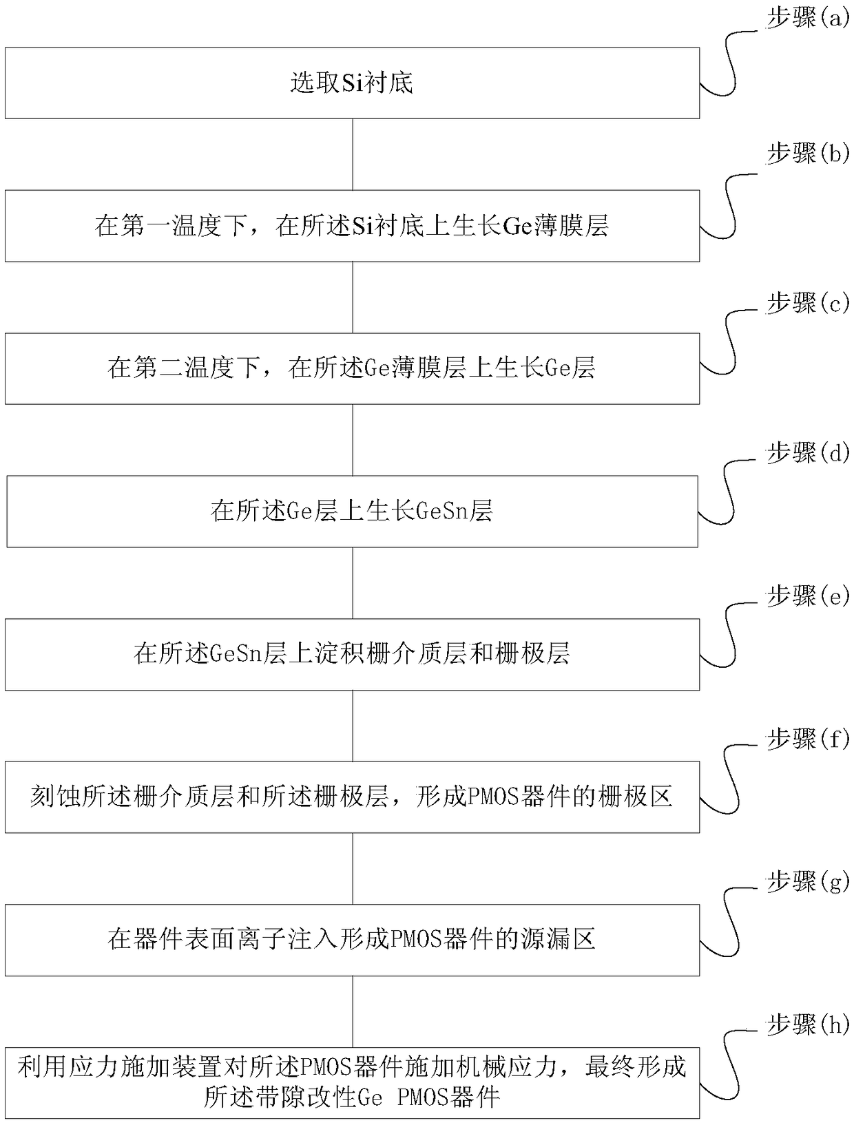
[0062] See figure 2 , figure 2 A flow chart of a method for preparing a direct bandgap Ge PMOS device provided by an embodiment of the present invention; the method includes the following steps:

[0063] Step a, select Si substrate;

[0064] Step b, growing a Ge thin film layer on the Si substrate at a first temperature;

[0065] Step c, growing a Ge layer on the Ge thin film layer at a second temperature;

[0066] Step d, growing a GeSn layer on the Ge layer;

[0067] Step e, depositing a gate dielectric layer and a gate layer on the GeSn layer;

[0068] Step f, etching the gate dielectric layer and the gate layer to form the gate region of the PMOS device;

[0069] Step g, forming source and drain regions of the PMOS device by ion implantation on the device surface;

[0070] Step h, using a stress applying device to apply mechanical stress to the PMOS device to finally form the bandgap modified Ge PMOS device.

[0071] Wherein, in step b and step c, the first temper...

Embodiment 2

[0089] See Figure 4a-Figure 4j , Figure 4a-Figure 4j It is a schematic diagram of a method for fabricating a direct bandgap Ge PMOS device provided by an embodiment of the present invention. On the basis of the above embodiments, this embodiment will introduce the process flow of the present invention in more detail. The method includes:

[0090] S101. Substrate selection. Such as Figure 4a As shown, the Si substrate sheet 201 whose crystal orientation is (001) is selected as the original material;

[0091] S102. Using the method of molecular beam epitaxy (MBE), on the Si substrate 201, grow an n-type Ge film with a crystal orientation of (001) on the Si substrate 201 by a two-step method of low temperature and high temperature, and the doping concentration is 1×10 16 ~5×10 16 cm -3 . specifically:

[0092] S1021, such as Figure 4b As shown, a 50 nm thick "low temperature" Ge ((LT-Ge) film 202 was grown at 275 ~ 325 °C. Most of the relaxation of elastic stress occur...


PUM


Abstract

The invention relates to a band-gap modified Ge PMOS device and a manufacturing method thereof. The manufacturing method comprises the steps of: selecting an Si substrate; growing a Ge thin film layer on the Si substrate at a first temperature; growing a Ge layer on the Ge thin film layer at a second temperature; growing a GeSn layer on the Ge layer; depositing a gate dielectric layer and a gate layer on the GeSn layer; etching the gate dielectric layer and the gate layer and forming a gate region; and carrying out ion implantation on the surface of the device to form a source-drain region, applying mechanical stress to a PMOS device by a stress applying device and finally forming the band-gap modified Ge PMOS device. A channel material utilized by the PMOS device is a direct band-gap modified Ge material; and the carrier mobility of the channel material is improved by multiple times in comparison with that of a traditional Si material, so that the current drive and frequency characteristics of the PMOS device are improved; and the device is suitable for monolithic optoelectronic integration with a photonic device.

Description

technical field [0001] The invention relates to the technical field of integrated circuits, in particular to a bandgap modified Ge PMOS device and a preparation method thereof. Background technique [0002] The "Moore's Law" that has had a huge impact on the development of the semiconductor industry: the number of transistors on an integrated circuit chip doubles about every 18 months, and the performance also doubles. For more than 40 years, the world semiconductor industry has been developing continuously according to this law. However, with the continuous reduction of device feature size, especially after entering the nanometer size, the development of microelectronic technology is getting closer and closer to the limit of materials, technology and devices, and is facing great challenges. When the feature size of the device is reduced to 65nm, the effects of short channel effect, strong field effect, quantum effect, parasitic parameters, and process parameter errors in n...

Claims


Application Information

Patent Timeline
Patent Type & Authority Patents(China)
IPC IPC(8): H01L21/336H01L21/58
Inventor 任远宋建军杨旻昱宣荣喜胡辉勇张鹤鸣
Owner XIDIAN UNIV
Why Eureka
Try Eureka