

Semiconductor/metal/semiconductor quantum well structure, preparation method and application thereof
A semiconductor and quantum well technology, applied in the field of semiconductor/metal/semiconductor quantum well structure, can solve the problems that cannot be realized and difficult to obtain high-quality semiconductor/metal/semiconductor epitaxial structure, and achieve the elimination of twins and high quality single crystal , the effect of reducing environmental noise
- Summary
- Abstract
- Description
- Claims
- Application Information
AI Technical Summary
Problems solved by technology
Method used
Image

Examples
Embodiment
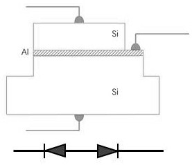
[0054] First, deoxidize the (111) crystal plane Si substrate, treat it with 8% hydrofluoric acid for 1 minute, the surface is hydrogen passivated surface, and then put it into the group IV molecular beam epitaxy equipment, at 900-1000 ℃ Under the condition of dehydrogenation treatment, a clean Si surface is obtained. The Si buffer layer can be grown on the Si surface, and the Si buffer layer can improve the surface flatness to a certain extent, thereby improving the surface flatness of subsequent film growth.
[0055] Next, an Al seed layer is grown under the condition of -50°C-50°C. The low-temperature growth and high-temperature annealing of the seed layer can obtain high-quality Al single crystal, which can be used as a template for subsequent epitaxial growth to ensure the quality of subsequent epitaxy.
[0056] The Al seed layer is heated at 100° C.-200° C. and annealed for 10-30 minutes.
[0057] Next, a layer of Al film with a thickness of 0.1-100nm is grown at a grow...
PUM
| Property | Measurement | Unit |
|---|---|---|
| Thickness | aaaaa | aaaaa |
Abstract
Description
Claims
Application Information