Manufacturing method of LTPS TFT based on metal induced crystallization process

A technology of metal-induced crystallization and manufacturing method, which is applied in the manufacture of semiconductor/solid-state devices, semiconductor devices, electrical components, etc., can solve the problems of large leakage current and large contact resistance of TFT devices, and reduce leakage current and contact resistance. The effect of impedance

Inactive Publication Date: 2016-10-12
SHENZHEN CHINA STAR OPTOELECTRONICS TECH CO LTD
View PDF4 Cites 15 Cited by
  • Summary
  • Abstract
  • Description
  • Claims
  • Application Information

AI Technical Summary

Benefits of technology

This technology allows creating lithography devices by controllably changing their electrical characteristics during production. By adding layers made of different materials or metals into this new material, it can improve its performance without affecting other components like transistors.

Problems solved by technology

This patented technical problem addressed in this patents relates to improving the performance of electronic displays that require thin films made from Low Temporary Solar Cell Materials (LTCF). Current methods involve depositing silicate glass onto an amorphous semiconductor called LPTF or forming it on top of another substrate like SiNx: These techniques result in poorly controlled thicknesses over time when producing these types of displays at reasonable costs. Additionally, some manufacturing processes may lead to contamination issues during deposition leading to reduced reliability.

Method used


Image

  • Manufacturing method of LTPS TFT based on metal induced crystallization process
  • Manufacturing method of LTPS TFT based on metal induced crystallization process
  • Manufacturing method of LTPS TFT based on metal induced crystallization process

Examples


Embodiment Construction

[0036] In order to further illustrate the technical means and effects adopted by the present invention, the following describes in detail in conjunction with preferred embodiments of the present invention and accompanying drawings.

[0037] see figure 1 , the present invention provides a method for manufacturing an LTPS TFT based on a metal-induced crystallization process, comprising the following steps:

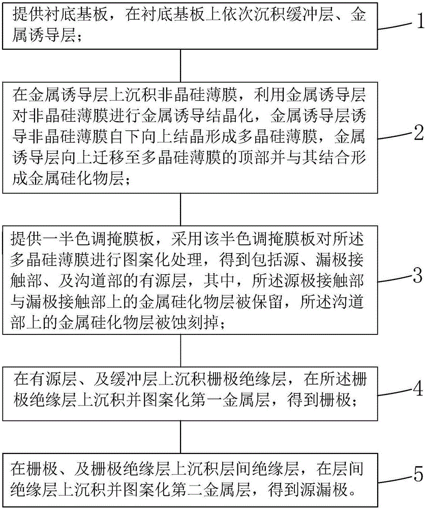
[0038] Step 1, such as figure 2 As shown, a base substrate 10 is provided, a buffer layer 20 is deposited on the base substrate 10 , and a metal inducing layer 35 is deposited on the buffer layer 20 .

[0039] Specifically, the thickness of the metal inducing layer 35 deposited in the step 1 is 5nm-10nm, and the material of the metal inducing layer 35 is nickel (Ni) or aluminum (Al).

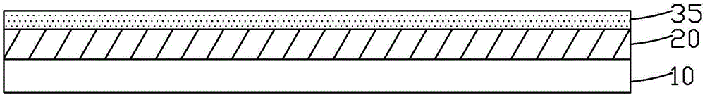
[0040] Step 2, such as Figure 3-4As shown, an amorphous silicon (a-Si) film 36 is deposited on the metal induction layer 35, and the metal induction layer 35 is used to carry out metal-in...


PUM

PropertyMeasurementUnit
Thicknessaaaaaaaaaa
Thicknessaaaaaaaaaa

Abstract

The invention provides a manufacturing method of an LTPS TFT based on a metal induced crystallization process. The manufacturing method comprises the steps of: forming a polycrystalline silicon thin film by adopting the metal induced crystallization process, wherein the top part of the polycrystalline silicon thin film is a metal silicide layer comprising a large number of metal ions and having an conductive property; adopting a halftone mask plate for carrying out patterning treatment on the polycrystalline silicon thin film to form an active layer, so that the metal silicide layer on a channel portion is etched away, and the purpose of reducing leakage current when the LTPS TFT is in an off state; and reserving the metal silicide layer on a source contact portion and a drain contact portion, thereby achieving the purposes of reducing contact resistance between the active layer and the source as well as the drain in the LTPS TFT.

Description


Claims


Application Information

Patent Timeline
Owner SHENZHEN CHINA STAR OPTOELECTRONICS TECH CO LTD
Why Eureka
Try Eureka