

Wafer-level packaging method for CMOS image sensor
An image sensor, wafer-level packaging technology, applied in the field of image sensors, can solve the problems of high thickness, high pixel product performance affecting image performance, etc., to achieve the effect of improving performance and reducing overall thickness
- Summary
- Abstract
- Description
- Claims
- Application Information
AI Technical Summary
Problems solved by technology
Method used
Image

Examples
Embodiment 1
[0024] Figure 1-Figure 10 It is a schematic diagram of the process of a wafer-level packaging method for a CMOS image sensor according to Embodiment 1 of the present invention.
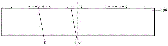
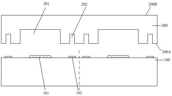
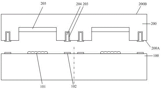
[0025] like figure 1 As shown, a first wafer 100 is provided, and the first wafer 100 has a plurality of image sensor chips, shown here as two adjacent image sensor chips, and the image sensor chips have dicing lines between each other (indicated by dot-dash line), the image sensor chip has a photosensitive area 101 and a non-photosensitive area, the photosensitive area has pixel units, and the non-photosensitive area has pads 102 .
[0026] like figure 2 As shown, a second wafer 200 is provided, and several first grooves 201 are formed on the first surface 200A of the second wafer 200, and the first grooves 201 correspond to the photosensitive region 101 of the image sensor; Several second grooves 202 are formed on the first surface 200A, and the second grooves 202 correspond to the bonding pads...
Embodiment 2
[0036] Figure 11-Figure 20 It is a schematic diagram of the process of the wafer-level packaging method of the CMOS image sensor according to the second embodiment of the present invention.
[0037] like Figure 11As shown, a first wafer 1100 is provided, the first wafer 1100 has a plurality of image sensor chips, here shown as two adjacent image sensor chips, the image sensor chips have dicing lines between each other (indicated by dot-dash line), the image sensor chip has a photosensitive area 1101 and a non-photosensitive area, the photosensitive area has pixel units, and the non-photosensitive area has pads 1102 .
[0038] like Figure 12 As shown, a second wafer 1200 is provided, and several first grooves 1201 are formed on the first surface 1200A of the second wafer 1200, and the first grooves 1201 correspond to the photosensitive regions 1101 of the image sensor; Several second grooves 1202 are formed on the first surface 1200A, and the second grooves 1202 correspon...
PUM
| Property | Measurement | Unit |
|---|---|---|
| Depth | aaaaa | aaaaa |
| Width | aaaaa | aaaaa |
| Depth | aaaaa | aaaaa |
Abstract
Description
Claims
Application Information