Terminal structure of super-junction semiconductor device

A technology of superjunction semiconductor and terminal structure, which is applied in semiconductor devices, electrical components, circuits, etc., can solve the problems of difficulty in reaching the withstand voltage value of device cells, low tolerance, and large difference between peak and valley values ​​of electric field. The effect of suppressing terminal charge imbalance, solving terminal withstand voltage problems, and simple and feasible process difficulty

Active Publication Date: 2016-10-12
UNIV OF ELECTRONICS SCI & TECH OF CHINA
View PDF2 Cites 4 Cited by
  • Summary
  • Abstract
  • Description
  • Claims
  • Application Information

AI Technical Summary

Problems solved by technology

However, the terminals of traditional super-junction devices continue to use PN strips with the same spacing as the cells to withstand the withstand voltage. This kind of PN strips has high doping concentration and small spacing, often with low tolerance. Depletion is prone to breakdown due to terminal charge imbalance
Mo...

Method used


Image

  • Terminal structure of super-junction semiconductor device
  • Terminal structure of super-junction semiconductor device
  • Terminal structure of super-junction semiconductor device

Examples


Embodiment Construction

[0021] Below in conjunction with accompanying drawing, describe technical scheme of the present invention in detail:

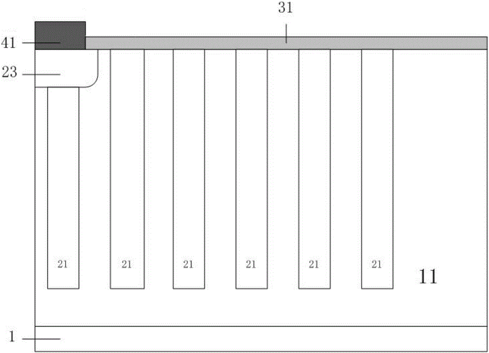
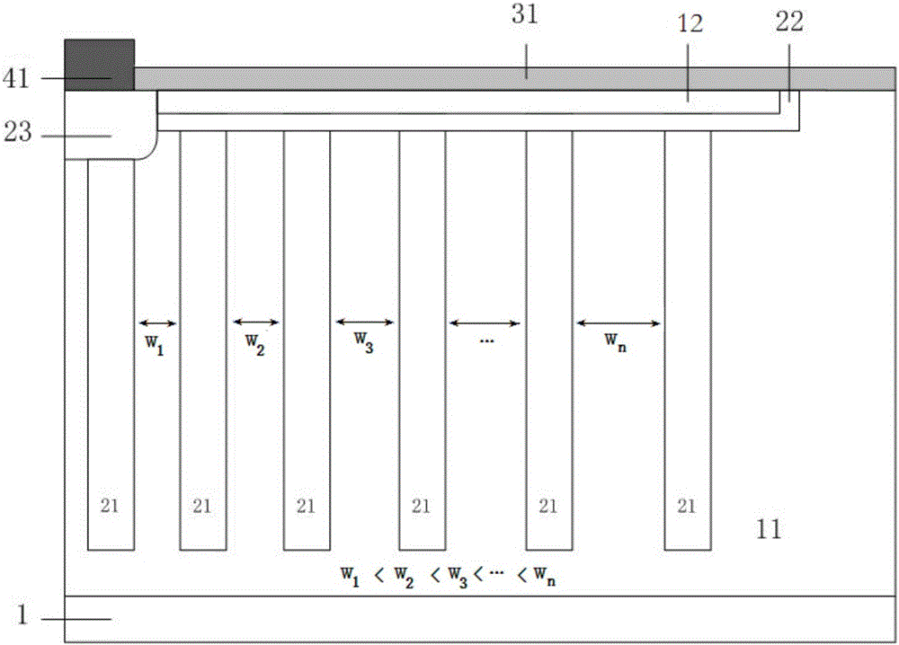
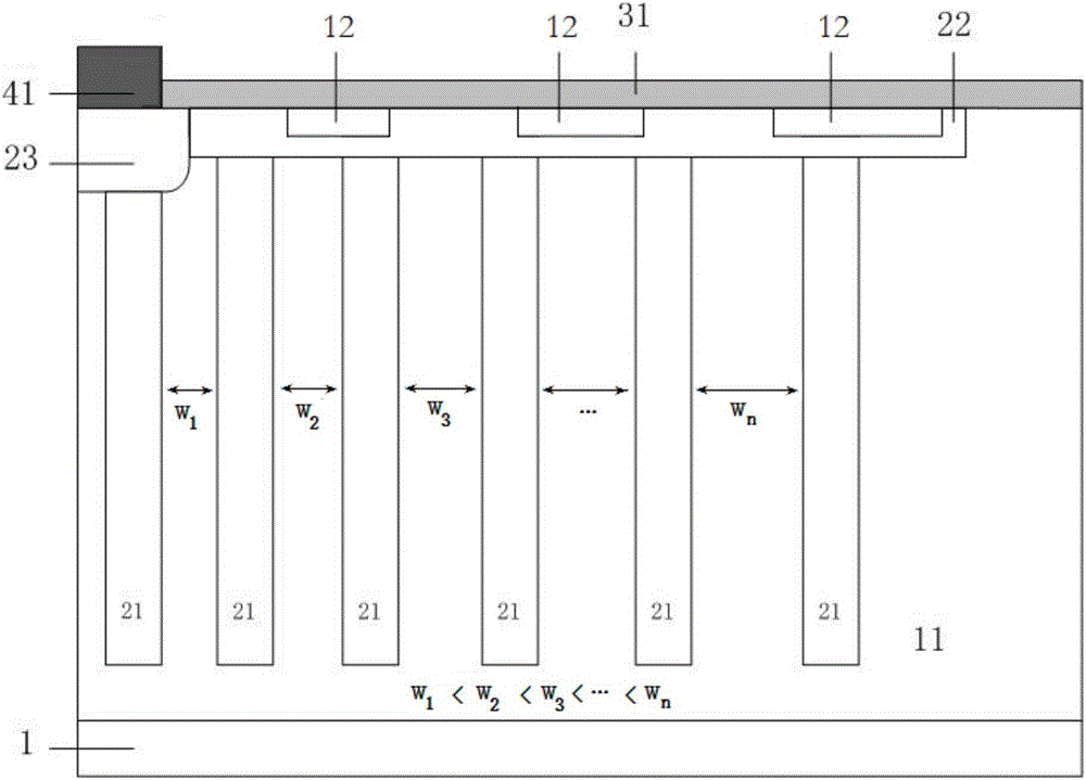
[0022] Such as figure 1 As shown, it is a sectional view of a terminal structure of a conventional superjunction vertical device, including a first conductivity type semiconductor substrate 1, a first conductivity type semiconductor drift region 11, a second conductivity type semiconductor drift region 21, a second conductivity type semiconductor Type cell region extension well 23, insulating layer 31, metal electrode 41; its first conductivity type semiconductor drift region 11 and second conductivity type semiconductor drift region 21 are on the first conductivity type semiconductor substrate 1, and mutually They are alternately and periodically arranged to form the device drift region together. The insulating layer 31 is located above the drift region, and the second conductivity type cell region extension well 23 is located between the insulating layer 31 ...


PUM


Abstract

The invention belongs to the technical field of a longitudinal super-junction semiconductor device, and specifically relates to a terminal structure of a super-junction semiconductor device. According to the terminal structure provided by the invention, the width of the first conductive type semiconductor drifting strip is adjustable, and the width is gradually changed from a cellular region to the boundary, so that the terminal charge can be well balanced so as to improve the voltage withstand of the device; next, a second conductive type surface doping region constantly covers a second conductive type semiconductor column, and extends towards the boundary for a certain distance so as to ensure that the border position of the two types of semiconductor drifting regions is fully covered to lower the surface peak electric field; and the first conductive type surface doping region in the second conductive type surface doping regions provides a positive charge center downwardly to further lower the surface electric field of the device so as to lower the probability of surface breakdown of the super-junction terminal in order to improve the overall voltage withstand of the device.

Description

technical field [0001] The invention belongs to the technical field of power semiconductor devices, and in particular relates to a terminal structure of a super junction semiconductor device. Background technique [0002] The proposal of the super junction breaks the silicon limit relationship between the traditional withstand voltage and the specific conductance to the power of 2.5, and the device has a lower specific on-resistance at the same time as the high withstand voltage. According to the superjunction theory, increasing the doping concentration of the PN strips in the drift region can effectively reduce the specific on-resistance of the device, and reducing the width of the PN strips can make the depletion between the PN strips more complete, thereby increasing the withstand voltage. Therefore, the cell design of most superjunction devices has the characteristics of high doping concentration and small stripe width. However, the terminals of traditional super-juncti...

Claims


Application Information

Patent Timeline
IPC IPC(8): H01L29/06
CPCH01L29/0634
Inventor 乔明章文通黄琬琰余洋张波
Owner UNIV OF ELECTRONICS SCI & TECH OF CHINA
Why Eureka
Try Eureka