One-step wet process black silicon preparation and surface treatment method

A technology of surface treatment and black silicon, which is applied in the field of solar cells, can solve problems affecting direct industrial application, increased leakage, and decreased open-circuit voltage of solar cells, so as to solve the bottleneck of mass industrialization, low battery leakage rate, and low cost. Effect

Active Publication Date: 2017-12-15
湖州叁峰能源新材料有限公司
View PDF2 Cites 0 Cited by
  • Summary
  • Abstract
  • Description
  • Claims
  • Application Information

AI Technical Summary

Problems solved by technology

[0010] However, the suede obtained by the above methods has a mixed structure of micron and nanometers, which has limitations in terms of uniformity and electrical properties.
In particular, there are serious defects in the surface treatment of black silicon, which leads to a decrease in the open circuit voltage of the solar cell and an increase in leakage, which directly affects the direct application of the industry.

Method used


Image

  • One-step wet process black silicon preparation and surface treatment method
  • One-step wet process black silicon preparation and surface treatment method
  • One-step wet process black silicon preparation and surface treatment method

Examples


Embodiment 1

[0057] Wet black silicon preparation and surface treatment method comprises the following steps:

[0058] (1) De-damage layer: Select a P-type polysilicon wafer (boron-doped, 1-3Qcm, 156X156mm square, thickness 180μm). Since the polysilicon wafer is cut with a diamond wire saw, it is necessary to perform alkali etching on the silicon wafer to remove damage layer;

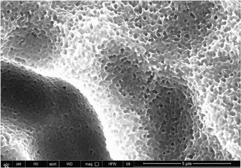
[0059] (2) Preparation of black silicon: Rinse the product wafer of step (1) with deionized water; after blowing dry, put it into the corrosion solution and react for 200 seconds at room temperature to prepare black silicon; wherein, the corrosion solution is metal ion-containing Mixed aqueous solution of concentrated hydrofluoric acid, oxidant and polymer; metal ions are derived from HAuCl 4 and AgNO 3 The combination of HAuCl4 and AgNO3 are electronic grade products, the weight ratio of HAuCl4 and AgNO3 is 1:6, the total content of HAuCl4 and AgNO3 in the solution is 0.01mol / L; the oxidant is hydrogen peroxide; ...

Embodiment 2

[0065] Wet black silicon preparation and surface treatment method comprises the following steps:

[0066] (1) De-damage layer: Select a P-type polysilicon wafer (boron-doped, 1-3Qcm, 156X156mm square, thickness 180μm). Since the polysilicon wafer is cut with a diamond wire saw, it is necessary to perform alkali etching on the silicon wafer to remove damage layer;

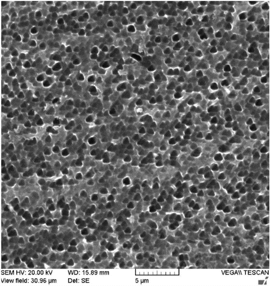
[0067] (2) Preparation of black silicon: Rinse the product wafer of step (1) with deionized water; after blowing dry, put it into the corrosion solution and react for 200 seconds at room temperature to prepare black silicon; wherein, the corrosion solution is metal ion-containing Mixed aqueous solution of concentrated hydrofluoric acid, oxidant and polymer; metal ions are derived from HAuCl 4 and AgNO 3 The combination of HAuCl4 and AgNO3 are electronic grade products, the weight ratio of HAuCl4 and AgNO3 is 1:5, the total content of HAuCl4 and AgNO3 in the solution is 0.007mol / L; the oxidant is hydrogen peroxide;...

Embodiment 3

[0073] Wet black silicon preparation and surface treatment method comprises the following steps:

[0074] (1) De-damage layer: Select a P-type polysilicon wafer (boron-doped, 1-3Qcm, 156X156mm square, thickness 180μm). Since the polysilicon wafer is cut with a diamond wire saw, it is necessary to perform alkali etching on the silicon wafer to remove damage layer;

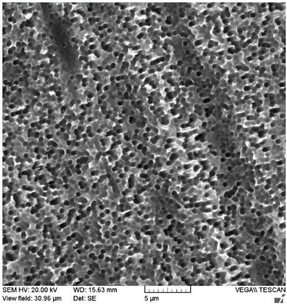
[0075] (2) Preparation of black silicon: Rinse the product wafer of step (1) with deionized water; after drying, put it into the corrosion solution and react for 300 seconds at 10°C to prepare black silicon; wherein, the corrosion solution contains metal ions The mixed aqueous solution of concentrated hydrofluoric acid, oxidant and high molecular polymer; the metal ion is derived from the combination of potassium chloroplatinate and palladium acetate, both of which are electronic grade products, potassium chloroplatinate and palladium acetate The weight ratio is 1:5, and the total content of potassium chloroplatina...


PUM

PropertyMeasurementUnit
reflectanceaaaaaaaaaa

Abstract

The invention provides a one-step wet black silicon preparation and surface treatment method, which includes the following steps: immersing the silicon wafer after removing the surface damage layer into an etching liquid and reacting to prepare black silicon; the etching liquid is concentrated hydrogen containing metal ions. A mixed aqueous solution of hydrofluoric acid, oxidant and high molecular polymer; the black silicon is immersed in the surface treatment etching liquid for surface optimization treatment, thereby obtaining a silicon wafer with a uniform texture of sub-micron structure; wherein, the surface treatment etching liquid contains Mixed acid aqueous solution of additives. The wet black silicon preparation method provided by the invention is simple in process and low in cost. The etched black silicon suede surface is uniform without sharp edges and has a reflectivity of 7-15%. This method greatly improves the absorption of light by silicon cells. Efficiency, solar cells made from black silicon produced by this method have lower cell leakage rate, stable open circuit voltage, and higher conversion efficiency.

Description

technical field [0001] The invention belongs to the field of solar cells, in particular to a one-step wet-process black silicon preparation and surface treatment method. Background technique [0002] The reflection of incident light on the surface of the silicon wafer greatly reduces the efficiency (current flow) of silicon solar cells. If the surface of the silicon cell is not treated with anti-reflection, about 40% of the sunlight will be lost. This antireflection effect must be effective across the entire solar spectrum and at a wide variety of incident light angles. [0003] Currently, antireflection on crystalline silicon photovoltaic cells is achieved through several different techniques. For monocrystalline silicon, anisotropic (pyramidal) texture etched silicon single crystals reduce reflectivity to about 5-15% above facing 100 monocrystalline silicon, but mainly at incident light angles close to 90° rather than reflection at low incidence angles At the same time,...

Claims


Application Information

Patent Timeline
Patent Type & Authority Patents(China)
IPC IPC(8): H01L31/18H01L31/0236C30B33/10
CPCC30B33/10H01L31/02363H01L31/1804Y02E10/547Y02P70/50
Inventor 韩庚欣丁晓辉韩冰徐涛
Owner 湖州叁峰能源新材料有限公司
Why Eureka
Try Eureka