

Semiconductor structure and formation method thereof
A technology of semiconductor and laminated structure, applied in the fields of semiconductor device, semiconductor/solid-state device manufacturing, electrical components, etc., can solve the problem that the electrical performance of semiconductor structure needs to be improved, etc.
- Summary
- Abstract
- Description
- Claims
- Application Information
AI Technical Summary
Problems solved by technology
Method used
Image

Examples
Embodiment Construction
[0027] The electrical performance of semiconductor structures formed according to the background art needs to be improved. figure 1 with figure 2 A structural schematic diagram showing the formation process of a semiconductor structure is now combined with figure 1 with figure 2 The reasons why the electrical performance of the semiconductor structure needs to be improved are analyzed.
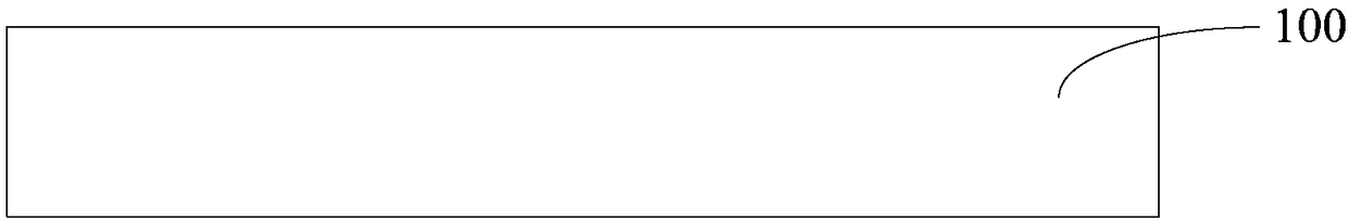
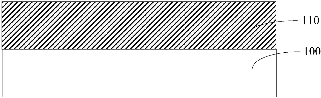
[0028] refer to figure 1 , providing substrate 100; using (NH 4 ) 2 The S solution performs sulfur doping treatment on the substrate 100 .
[0029] refer to figure 2 , using (NH 4 ) 2 After the sulfur doping treatment is performed on the substrate 100 by the S solution, a dielectric layer 110 is formed on the substrate 100 .
[0030] The electrical performance of the semiconductor structure formed by the above forming method needs to be improved.
[0031] After analysis, it is found that the reasons for the electrical performance of the semiconductor structure to be improved in...
PUM
 Abstract
Description
Claims
Application Information