

Epitaxial structure provided with Bragg reflector, preparation method thereof and LED chip
A Bragg reflector and epitaxial structure technology, applied in electrical components, circuits, semiconductor devices, etc., can solve the problem of low light-emitting efficiency of LED chips, and achieve the effect of improving anti-static ability, improving overall yield, and simplifying process
- Summary
- Abstract
- Description
- Claims
- Application Information
AI Technical Summary
Problems solved by technology
Method used
Image

Examples
preparation example Construction
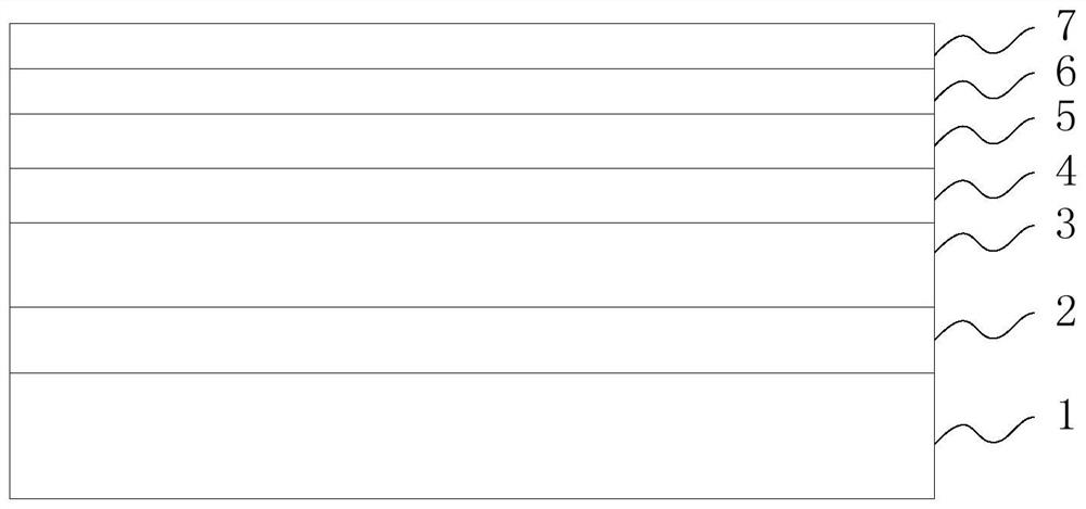
[0061] Correspondingly, the present application also provides a method for preparing an epitaxial structure provided with a Bragg mirror, comprising the following steps:
[0062] S1. Forming a GaN composite layer on the substrate by metal-organic compound chemical vapor deposition;
[0063] Specifically, the preparation method of the GaN composite layer includes:
[0064] Forming a GaN buffer layer with a thickness of 10-100 nm on the substrate under the conditions of a temperature of 500-900° C. and a pressure of 180-220 Torr;
[0065] Raise the temperature to 900-1200° C., keep the pressure constant, and form a GaN non-doped layer with a thickness of 2-4 μm on the GaN buffer layer.
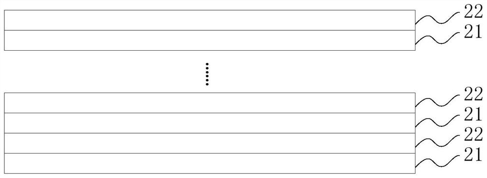
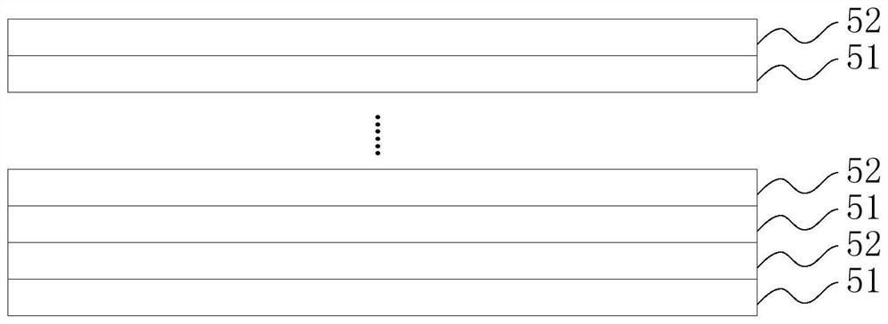
[0066] S2. Under the conditions of a temperature of 900-1200° C. and a pressure of 180-220 Torr, several periods of AlN layers / GaN layers are formed on the GaN composite layer to form a Bragg reflector;
[0067] S3. Keeping the temperature and pressure constant, forming an N-GaN layer on the B...
Embodiment 1
[0081] A method for preparing an epitaxial structure provided with a Bragg reflector, comprising the following steps:
[0082] S1. Adjust the temperature in the reaction chamber to 1050° C., and maintain the pressure in a hydrogen atmosphere to process the sapphire substrate for 2 minutes;
[0083] S2. Lower the temperature to 555° C., maintain the pressure at 500 Torr, and form a GaN buffer layer with a thickness of 40 nm on the sapphire substrate;
[0084] S3, raising the temperature to 1050° C., maintaining the pressure at 200 Torr, and forming a GaN undoped layer with a thickness of 3 μm on the GaN buffer layer;
[0085]S4. Keeping the temperature and pressure constant, grow 30 cycles of AlN layer and GaN layer on the GaN undoped layer to form a Bragg mirror, and the thickness of the AlN layer and GaN layer in each cycle is 30nm and 48.5nm;
[0086] S5. Keeping the temperature and pressure constant, an N-GaN layer with a thickness of 2 μm is formed on the Bragg reflector,...
Embodiment 2
[0094] A method for preparing an epitaxial structure provided with a Bragg reflector, comprising the following steps:
[0095] S1. Adjust the temperature in the reaction chamber to 1050° C., and maintain the pressure in a hydrogen atmosphere to process the sapphire substrate for 2 minutes;
[0096] S2. Lower the temperature to 800° C., maintain the pressure at 600 Torr, and form a GaN buffer layer with a thickness of 70 nm on the sapphire substrate;
[0097] S3, raising the temperature to 1150° C., maintaining the pressure at 220 Torr, and forming a GaN undoped layer with a thickness of 4 μm on the GaN buffer layer;
[0098] S4. Keeping the temperature and pressure constant, grow 25 cycles of AlN layer and GaN layer on the GaN undoped layer to form a Bragg reflector, and the thickness of the AlN layer and GaN layer in each cycle is 32nm and 52nm;
[0099] S5. Keeping the temperature and pressure constant, an N-GaN layer with a thickness of 3 μm is formed on the Bragg reflecto...
PUM
| Property | Measurement | Unit |
|---|---|---|
| Thickness | aaaaa | aaaaa |
| Thickness | aaaaa | aaaaa |
| Thickness | aaaaa | aaaaa |
Abstract
Description
Claims
Application Information