LED epitaxial wafer with current blocking layer and manufacturing method thereof

A technology of LED epitaxial wafer and current blocking layer, which is applied in the direction of circuits, electrical components, semiconductor devices, etc., can solve the problems of LED failure and no current around the electrode, and achieve the effect of preventing excessive concentration

Active Publication Date: 2016-10-12
NANTONG YIXUAN IND DESIGN CO LTD
View PDF3 Cites 6 Cited by
  • Summary
  • Abstract
  • Description
  • Claims
  • Application Information

AI Technical Summary

Problems solved by technology

[0002] The semiconductor light-emitting elements currently used are mainly LEDs (light-emitting diodes). LED epitaxial wafers generally grow electrodes directly on top of the current expansion layer. At this time, due to the limited position of the electrodes, most of the current will be concentrated below the electrodes. As a result, there is no current around the electrode, and the excessive concentration of this current will generate a lot of heat, which will eventually lead to the failure of the LED

Method used


Image

  • LED epitaxial wafer with current blocking layer and manufacturing method thereof
  • LED epitaxial wafer with current blocking layer and manufacturing method thereof
  • LED epitaxial wafer with current blocking layer and manufacturing method thereof

Examples


Embodiment Construction

[0026] see Figure 1-8 , the present invention at first provides a kind of manufacturing method of the LED epitaxial wafer with current blocking layer, specifically comprises the following steps:

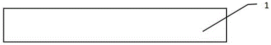
[0027] see figure 1 , providing a substrate 1, the substrate 1 is a sapphire substrate;

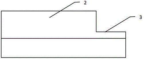
[0028] see figure 2 , growing a GaN epitaxial layer 2 on the substrate 1: sequentially growing a silicon-doped N-type GaN layer, a multi-quantum well light-emitting layer, and a magnesium-doped P-type GaN layer on the substrate 1; and then etching by dry etching Out of the first electrode placement area 3, the placement area is stepped;

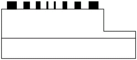
[0029] see image 3 , forming a photoresist layer 4 in the unetched region of the GaN epitaxial layer 2;

[0030] see Figure 4 , etch the photoresist layer 4 to form a series of concentric rings; fill the concentric rings with ITO to form a conductive ring 5, the center of the conductive ring 5 is connected to the unetched region of the GaN epitaxial ...


PUM


Abstract

The invention provides an LED epitaxial wafer with a current blocking layer. The LED epitaxial wafer comprises a substrate. A GaN epitaxial layer is epitaxially grown on the substrate. Dry method etching is used to etch a first electrode placing area which is in the shape of a ladder. A current barrier layer is formed on the non-etched area of the GaN epitaxial layer. Concentric ITO conductive rings are uniformly spaced in the current barrier layer. The top surfaces of the conductive rings are level with the top surface of the current barrier layer. An ITO current expansion layer is deposited on the current barrier layer. According to the invention, the concentric conductive rings are used to transfer current, and the excessive concentration of the current in the middle of an electrode is prevented.

Description

technical field [0001] The invention relates to the field of semiconductor light emitting, in particular to an LED epitaxial wafer with a current blocking layer and a manufacturing method thereof. Background technique [0002] The semiconductor light-emitting elements currently used are mainly LEDs (light-emitting diodes). LED epitaxial wafers generally grow electrodes directly on top of the current expansion layer. At this time, due to the limited position of the electrodes, most of the current will be concentrated below the electrodes. As a result, there is no current around the electrode, and the excessive concentration of this current will generate a lot of heat, which will eventually lead to the failure of the LED. Contents of the invention [0003] Based on solving the problems in the above packaging, the present invention provides a method for manufacturing an LED epitaxial wafer with a current blocking layer, which specifically includes the following steps: [000...

Claims


Application Information

Patent Timeline
Patent Type & Authority Applications(China)
IPC IPC(8): H01L33/00H01L33/14H01L33/46
CPCH01L33/007H01L33/145H01L33/46
Inventor 王汉清
Owner NANTONG YIXUAN IND DESIGN CO LTD
Why Eureka
Try Eureka