Metal contamination immediate monitoring method of semiconductor wafer

A semiconductor and wafer technology, applied in the monitoring field of semiconductor manufacturing process, can solve problems such as measurement error, misjudgment, reduced lifespan or diffusion length measurement value, etc., to achieve the effect of reducing production cost

Inactive Publication Date: 2016-10-19
POWERCHIP TECH CORP
View PDF3 Cites 1 Cited by
  • Summary
  • Abstract
  • Description
  • Claims
  • Application Information

AI Technical Summary

Problems solved by technology

However, metal contamination of semiconductor wafers reduces the measured value of lifetime or diffusion length, and the above-mentioned BMD or microscopic defects also reduce the measured value of lifetime or diffusion length
Therefore, the BMD or tiny defects in the semiconductor wafer and the state of the wafer surface will affect the measured value of the diffusion length measured by the surface photovoltage, which will make the measured value wrong and cause a misjudgment of whether the metal is contaminated or not.

Method used


Image

  • Metal contamination immediate monitoring method of semiconductor wafer
  • Metal contamination immediate monitoring method of semiconductor wafer
  • Metal contamination immediate monitoring method of semiconductor wafer

Examples


Embodiment Construction

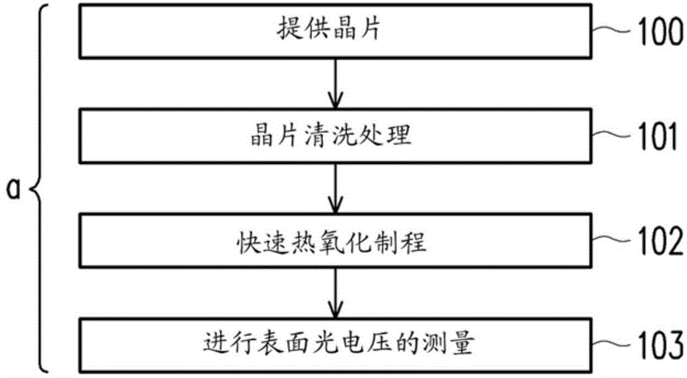
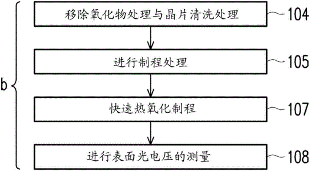
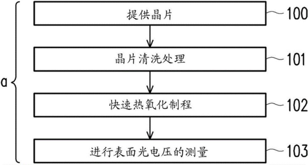
[0031] The method for real-time monitoring of metal contamination of semiconductor wafers of the present invention can be divided into low-temperature processing and high-temperature processing according to the processing temperature. Wherein, the metal pollution real-time monitoring method of the semiconductor wafer can be used to monitor the metal pollution of the following machines: 1. Low-temperature process machine: yellow light machine, etching machine, wet etching machine, ion implantation machine etc.; 2. High-temperature process machines: furnace tube machines, rapid annealing machines, physical vapor deposition machines, chemical vapor deposition machines, etc.

[0032] Hereinafter, a method for real-time monitoring of metal contamination of a semiconductor wafer according to an embodiment of the present invention is described, which is used in a low-temperature process.

[0033] Figure 1A and Figure 1B It is a flow chart of a method for real-time monitoring of me...


PUM


Abstract

A metal contamination immediate monitoring method of a semiconductor wafer is provided to include: performing a rapid thermal oxidation process on the wafer; and performing surface photo-voltage measurement on the wafer after the rapid thermal oxidation process.

Description

technical field [0001] The present invention relates to a monitoring method of a semiconductor manufacturing process, and in particular to a real-time monitoring method of metal contamination of a semiconductor wafer. Background technique [0002] In the semiconductor manufacturing process, the metal contamination of the wafer will have an adverse effect on the device characteristics of the product. For example, heat treatment of the product will allow heavy metals such as iron (Fe) or nickel (Ni) to enter the silicon wafer through diffusion, and form a deep energy level in the band gap to serve as a carrier capture center or The recombination centers cause pn junction leaks and life reduction in the device. Therefore, in order to monitor the degree of metal contamination in the manufacturing process, a monitoring method capable of real-time monitoring and high reliability is sought. [0003] In the image sensor, the tolerance to metal is limited, and if it is contaminated...

Claims


Application Information

Patent Timeline
IPC IPC(8): H01L21/66
Inventor 蔡家欣廖曼钧林钰淇江烨瑜
Owner POWERCHIP TECH CORP
Why Eureka
Try Eureka