Preparation method for GaInP/GaAs dual-junction solar cell

A technology for solar cells and bottom cells, applied in the field of solar cells, can solve problems such as GaAs damage, difficult to control the accuracy of components, and complex preparation processes

Inactive Publication Date: 2016-10-19
SUZHOU INST OF NANO TECH & NANO BIONICS CHINESE ACEDEMY OF SCI
View PDF6 Cites 0 Cited by
  • Summary
  • Abstract
  • Description
  • Claims
  • Application Information

AI Technical Summary

Problems solved by technology

[0003] At present, there are two main methods for making III-V multi-junction cells on Si substrates. One is to grow GaInP/GaAs double-junction cells on GaAs substrates first, and then bond the cells to Si substrates. It is relatively complicated, and the use of wet etching will cause damage to GaAs; in addition, the preparation process for bonding and the process of stripping the GaAs substrate must have high production capacity and equipment to effectively reduce costs
The second is to directly grow double-junction ce

Method used


Image

  • Preparation method for GaInP/GaAs dual-junction solar cell
  • Preparation method for GaInP/GaAs dual-junction solar cell
  • Preparation method for GaInP/GaAs dual-junction solar cell

Examples


Embodiment Construction

[0024] Hereinafter, embodiments of the present invention will be described in detail with reference to the accompanying drawings. This invention may, however, be embodied in many different forms and should not be construed as limited to the specific embodiments set forth herein. Rather, the embodiments are provided to explain the principles of the invention and its practical application, thereby enabling others skilled in the art to understand the invention for various embodiments and with various modifications as are suited to particular intended uses. In the drawings, the shapes and dimensions of elements may be exaggerated for clarity, and the same reference numerals will be used throughout to designate the same or like elements.

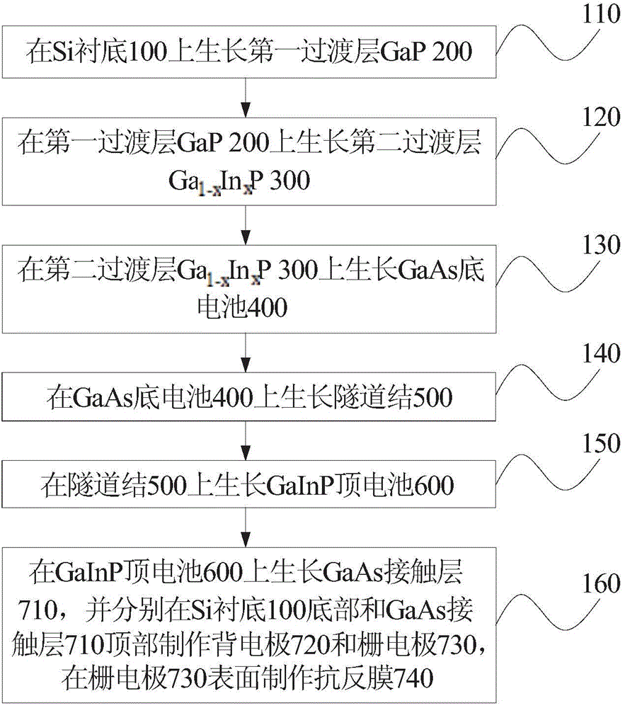
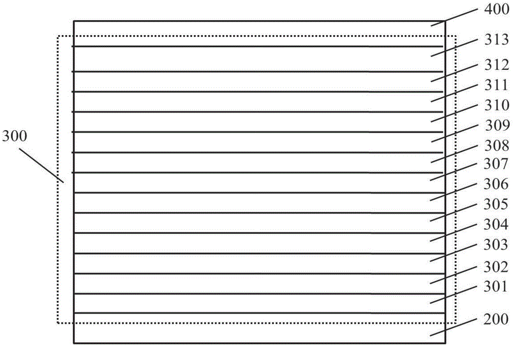
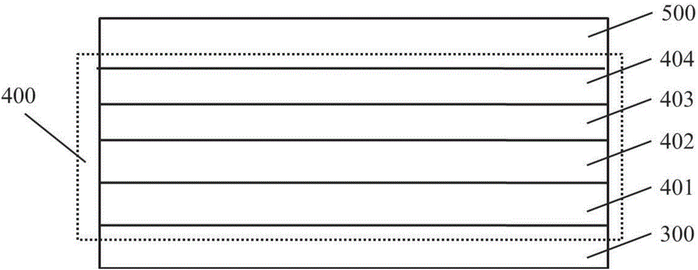
[0025] figure 1 It is a flowchart of steps of a method for preparing a GaInP / GaAs double-junction solar cell according to an embodiment of the present invention.

[0026] refer to figure 1 , The method for preparing a GaInP / GaAs double-junctio...


PUM

PropertyMeasurementUnit
Thicknessaaaaaaaaaa

Abstract

The invention discloses a preparation method for a GaInP/GaAs dual-junction solar cell. The preparation method comprises: step A, a first transition layer GaP grows on a substrate; step B, a second transition layer Ga(1-x)InxP grows on the first transition layer GaP; step C, a GaAs bottom cell grows on the second transition layer Ga(1-x)InxP; and step D, a GaInP top cell grows on the GaAs bottom cell, wherein the content of indium in the second transition layer Ga(1-x)InxP is adjusted to realize matching of the lattice constant of the second transition layer Ga(1-x)InxP with the lattice constant of the GaAs bottom cell. According to the preparation method, the GaP and the Ga(1-x)InxP are used as transition layers and transition of the lattice constant of the second transition layer Ga(1-x)InxP to the lattice constant of the GaAs bottom cell is realized, so that lattice constant matching is realized and thus an objective of growing and preparing a GaInP/GaAs dual-junction solar cell is achieved.

Description

technical field [0001] The invention belongs to the field of solar cells, and in particular relates to a preparation method of a GaInP / GaAs double-junction solar cell. Background technique [0002] Environmental and energy requirements make new energy technologies, including solar energy efficient power generation, more and more important. As a forward-looking and strategic new clean energy technology that supports the sustainable development of my country's national economy, high-efficiency solar power generation technology is listed as a key support and priority development direction in the national medium and long-term scientific and technological development plan. Multi-junction III-V compound semiconductor solar cells use various semiconductor materials with different bandgap widths to absorb the part of sunlight that matches their bandgap widths, thereby achieving broad-spectrum absorption of sunlight. At present, the efficiency of double-junction cells has reached Ex...

Claims


Application Information

Patent Timeline
IPC IPC(8): H01L31/18
CPCY02P70/50
Inventor 代盼陆书龙季莲吴渊渊谭明杨辉
Owner SUZHOU INST OF NANO TECH & NANO BIONICS CHINESE ACEDEMY OF SCI
Why Eureka
Try Eureka