

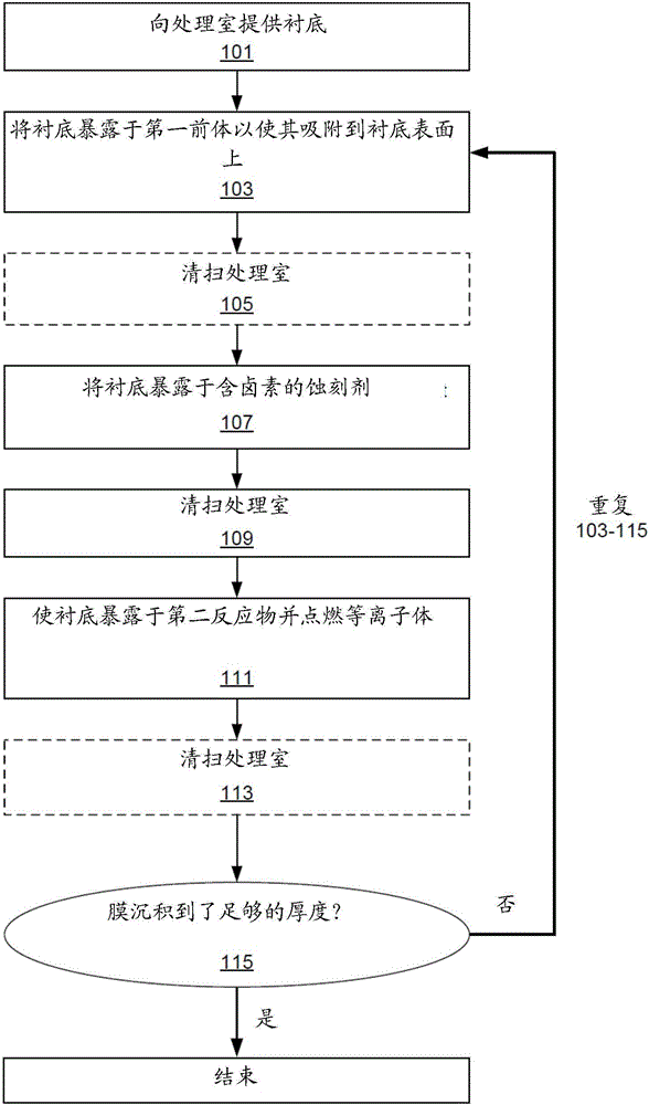
Deposition of conformal films by atomic layer deposition and atomic layer etch
A technology of etchant and adsorption layer, applied in the fields of atomic layer deposition and atomic layer etching deposition conformal film
- Summary
- Abstract
- Description
- Claims
- Application Information
AI Technical Summary
Problems solved by technology
Method used
Image

Examples
Embodiment Construction
[0062] In the following description, numerous specific details are set forth in order to provide a thorough understanding of the presented embodiments. The disclosed embodiments may be practiced without some or all of these specific details. In other instances, well known process operations have not been described in detail to avoid unnecessarily obscuring the disclosed embodiments. While the disclosed embodiments will be described in conjunction with specific embodiments, it will be understood that no limitation to the disclosed embodiments is intended.
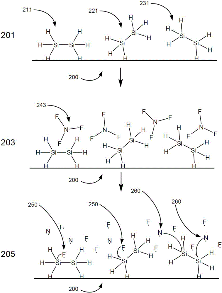
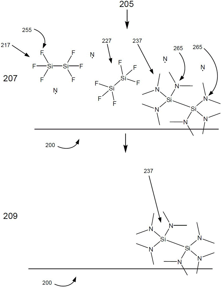
[0063] The implementations disclosed below describe the deposition of materials on substrates such as wafers or other workpieces. Workpieces can be of various shapes, sizes, and materials. In addition to semiconductor wafers, other workpieces that may be used in implementations of the present disclosure include various items such as printed circuit boards and the like. The process and apparatus can be used in the manufact...
PUM
| Property | Measurement | Unit |
|---|---|---|
| Opening diameter | aaaaa | aaaaa |
| Width | aaaaa | aaaaa |
Abstract
Description
Claims
Application Information