an alignment jig

A jig and ring frame technology, applied in the direction of manufacturing tools, auxiliary devices, auxiliary welding equipment, etc., can solve problems such as unfavorable mass production, difficult circuit boards, difficult welding, etc., to achieve convenient operation, simple structure, and avoid offset Effect

Active Publication Date: 2017-11-24
SHENZHEN INST OF ADVANCED TECH CHINESE ACAD OF SCI
View PDF5 Cites 0 Cited by
  • Summary
  • Abstract
  • Description
  • Claims
  • Application Information

AI Technical Summary

Problems solved by technology

[0002] In the preparation process of the fully wired ultrasonic probe, the piezoelectric array element is connected to the cable through the circuit board to form a connection loop, and the piezoelectric array element and the circuit board can be connected in two ways: 1. Welding on each array element The piezoelectric array elements are connected to the circuit board through welding wires. With this connection method, when the number of piezoelectric array elements is large, welding will be difficult and time-consuming, which is not conducive to mass production; 2. A plurality of circuit boards form an array corresponding to each array element of the piezoelectric array element one by one. The array and the piezoelectric array element are aligned with each other, and the terminals on the circuit board form an electrical connection with the piezoelectric array element. The second This connection method is easier to operate than the first connection method, which is conducive to mass production, but when the second connection method is used, when the number of piezoelectric elements is large, each piezoelectric element is small, and it is difficult for the circuit board to be connected to the circuit board. The piezoelectric array elements are precisely aligned, and a slight misalignment will cause a large number of array elements to fail to conduct with the circuit board, and the ultrasonic probe will be scrapped. Therefore, solving the alignment problem between the circuit board and the piezoelectric array element is the second connection The key to the smooth implementation of the method

Method used


Image

  • an alignment jig
  • an alignment jig
  • an alignment jig

Examples


Embodiment Construction

[0024] In order to have a clearer understanding of the technical features, purposes and effects of the present invention, the specific implementation manners of the present invention will now be described with reference to the accompanying drawings.

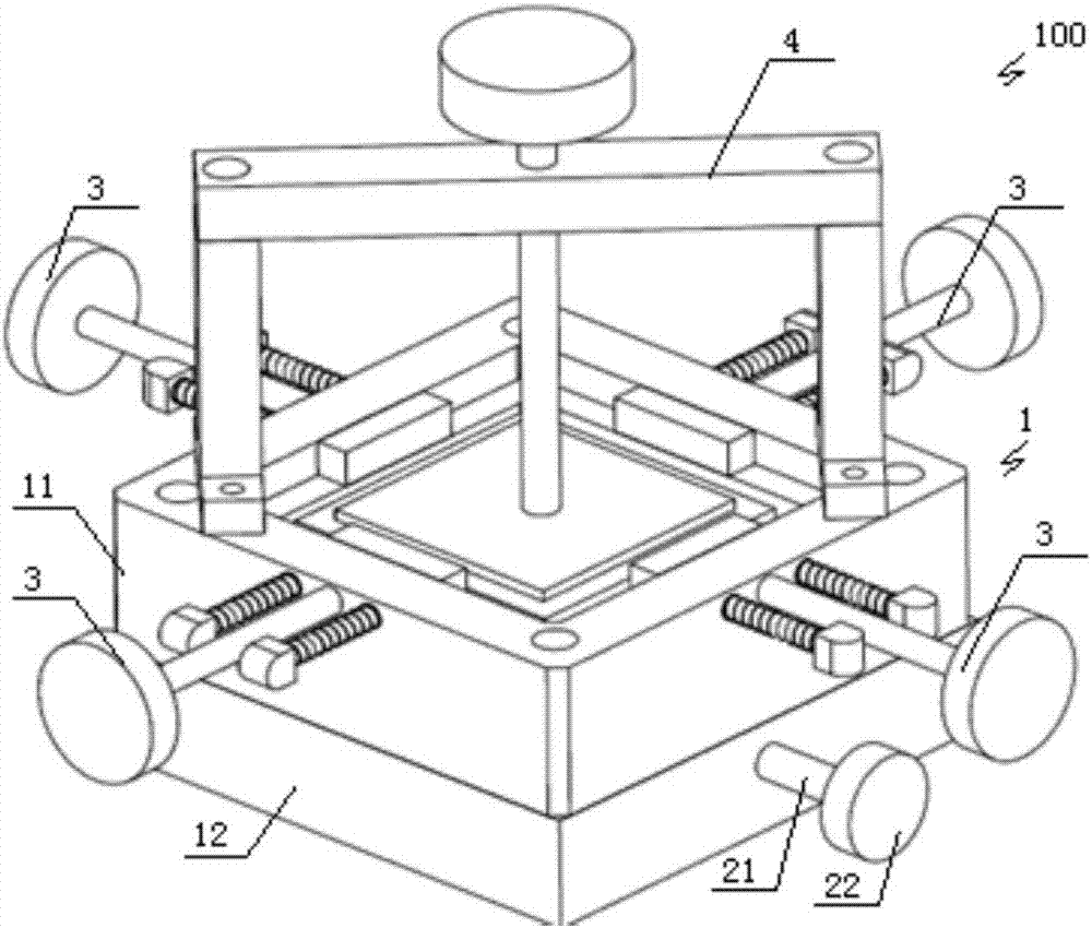
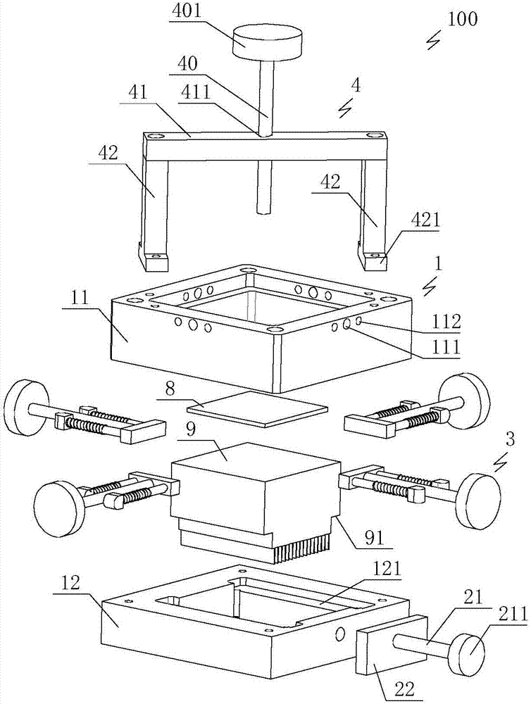
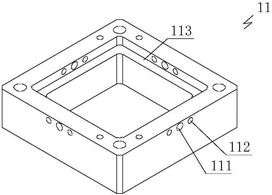
[0025] Such as Figure 1a , Figure 1b As shown, an alignment fixture 100 provided by the present invention includes an annular frame 1, on which a positioning mechanism for fixing a backing 9 containing a circuit board array is arranged. In this embodiment, a plurality of circuit boards The formed circuit board array and the backing 9 are molded by casting, so that the ends (the prior art, not shown in the figure) aligned between the circuit board and the piezoelectric array element 8 form an array corresponding to the piezoelectric array element 8 one-to-one , and then polish the pouring surface to expose the terminal array (copper core array, prior art, not shown in the figure), and the connection between the terminal copper c...


PUM


Abstract

The invention discloses an aligning jig which comprises a annular frame, and a positioning mechanism used for fixing a back lining comprising a circuit board array is arranged on the annular frame; a regulating mechanism used for regulating a piezoelectric array element is arranged in the position, above the positioning mechanism, of the annular frame; and a pressing mechanism used for pressing the piezoelectric array element and the back lining is arranged above the top of the annular frame. The aligning jig solves the problem of alignment of the circuit board and the piezoelectric array element, is simple to operate, and is precise in positioning.

Description

technical field [0001] The invention relates to the technical field of circuit board connection, in particular to an alignment jig used for precise alignment of a piezoelectric array element and a circuit board. Background technique [0002] In the preparation process of the fully wired ultrasonic probe, the piezoelectric array element is connected to the cable through the circuit board to form a connection loop, and the piezoelectric array element and the circuit board can be connected in two ways: 1. Welding on each array element The piezoelectric array elements are connected to the circuit board through welding wires. With this connection method, when the number of piezoelectric array elements is large, welding will be difficult and time-consuming, which is not conducive to mass production; 2. A plurality of circuit boards form an array corresponding to each array element of the piezoelectric array element one by one. The array and the piezoelectric array element are alig...

Claims


Application Information

Patent Timeline
Patent Type & Authority Patents(China)
IPC IPC(8): B23K37/047
CPCB23K37/047B23K2101/42
Inventor 李永川钱明黄继卿何华林郑海荣
Owner SHENZHEN INST OF ADVANCED TECH CHINESE ACAD OF SCI
Why Eureka
Try Eureka