Thin-film transistor array substrate, display panel and display device

A technology for thin film transistors and array substrates, applied in the display field, can solve the problems of low cell thickness, easy sliding of photoresist material isolation columns into PLN holes, scratches on alignment films, etc., to achieve good inversion effect, improve display quality, and The effect of surface pressure

Active Publication Date: 2016-11-09
XIAMEN TIANMA MICRO ELECTRONICS +1
View PDF4 Cites 1 Cited by
  • Summary
  • Abstract
  • Description
  • Claims
  • Application Information

AI Technical Summary

Problems solved by technology

[0004] When the size of each sub-pixel is reduced in order to increase the pixel display density of the LCD, the PLN holes need to maintain the original size due to process limitations, so that the distance between adjacent PLN holes is relatively close, which will lead to isolation of the photoresist material If there is an arc at the support position where the column is located, the photoresist material isolation column cannot be in full contact with the lower substrate. When the vacuum bonding is poor, the photoresist material isolation column is easy to slide into the PLN hole, resulting in The thickness of the cell at the location of the material isolation column is relatively low; moreover, during manual operation, the sliding of the photoresist material isolation column can easily lead to scratches on the alignment film

Method used


Image

  • Thin-film transistor array substrate, display panel and display device
  • Thin-film transistor array substrate, display panel and display device
  • Thin-film transistor array substrate, display panel and display device

Examples


Embodiment Construction

[0046] In order to make the purpose, technical solutions and advantages of the present invention clearer, the present invention will be further described in detail below in conjunction with the accompanying drawings. Obviously, the described embodiments are only some of the embodiments of the present invention, rather than all of them. Based on the embodiments of the present invention, all other embodiments obtained by persons of ordinary skill in the art without making creative efforts belong to the protection scope of the present invention.

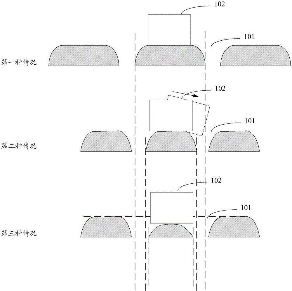
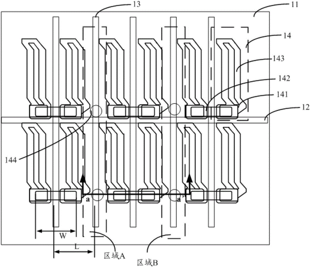
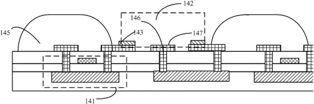
[0047] When reducing the size of each pixel unit in order to increase the pixel display density of the LCD, due to process limitations, the through hole needs to maintain the original size, such as figure 1 shown in the second case. At this time, due to the short distance between the adjacent through holes 101, when the through holes are formed by etching, an arc will appear at the supporting position where the spacer column 102 is loca...


PUM


Abstract

The invention discloses a thin-film transistor array substrate, a display panel and a display device. The thin-film transistor array substrate mainly comprises the components of a substrate; a plurality of gate wires and data wires which are arranged on the substrate and are crossed with and insulated from one another; and a plurality of pixel units which are arranged in an area that is defined by the gate wires and the data wires, wherein each pixel unit comprises a switch element; an insulating layer which is arranged on the switch element and is provided with a through hole; and a pixel electrode which is arranged on the insulating layer and is electrically connected with the switch element through the through hole, wherein two pixel units which are adjacent in the extending direction of the gate wires share one through hole, so that a large-enough distance between the two through holes which are adjacent in the transverse direction is realized, thereby well placing insulating columns, thereby preventing problems of low standing stability and easy slippage of the insulating columns, and furthermore ensuring high thickness uniformity and relatively high surface pressure resistance.

Description

[0001] The application of the present invention is a divisional application of the invention application with the filing date of June 5, 2014, the application number of 201410246489.0, and the title of the invention "A Thin Film Transistor Array Substrate, Display Panel and Display Device". technical field [0002] The invention relates to the field of display technology, in particular to a thin film transistor array substrate, a display panel and a display device. Background technique [0003] In the existing liquid crystal display (Liquid Crystal Display, LCD) pixel structure, especially for the pixel structure in In-Plane Switching (In-Plane Switching, IPS) and Fringe Field Switching (Fringe Field Switching, FFS) mode, in order to make The electric field is uniform in the horizontal direction, and a planarization layer (Planarization, PLN) will be formed before forming the pixel electrodes. And form uniformly distributed through holes 101 in the PLN layer (such as figure...

Claims


Application Information

Patent Timeline
Patent Type & Authority Applications(China)
IPC IPC(8): H01L27/12G02F1/1362
CPCG02F1/136227G02F1/136286H01L27/124H01L27/1248G02F1/13685H10K59/123H01L29/78663H01L29/78672H01L29/7869G02F1/1368
Inventor 李伟平
Owner XIAMEN TIANMA MICRO ELECTRONICS
Why Eureka
Try Eureka