Producing method for P-trench VDMOS device
A production method and device technology, applied in the fields of semiconductor devices, semiconductor/solid-state device manufacturing, electrical components, etc., can solve the problems of positive oxide charge accumulation, large Vth, Vth becoming large, etc., to achieve performance improvement, avoid negative Affect, reduce the effect of positive charge
- Summary
- Abstract
- Description
- Claims
- Application Information
AI Technical Summary
Problems solved by technology
Method used
Image
Examples
Embodiment Construction
[0028] A kind of P channel VDMOS device production method, comprises the steps:
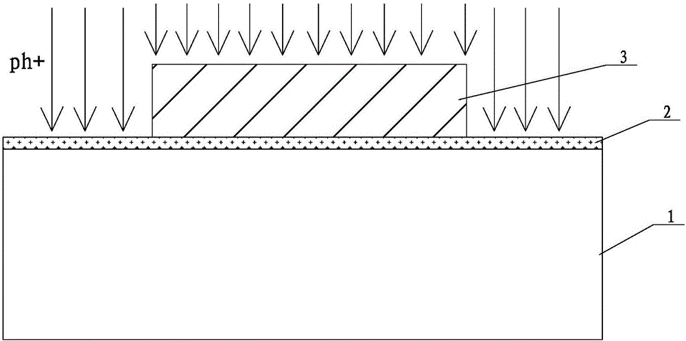
[0029] Step 1), after the active area of the epitaxial layer 1 is opened, thin oxygen growth is performed first to form the oxide layer 2, and then the photoresist layer 3 is covered on the oxide layer 2, and the glue is partially removed according to the design requirements, and then the polycrystalline gate is used The photolithography plate is injected with N-type impurities (ph+) with glue, such as figure 1 shown;
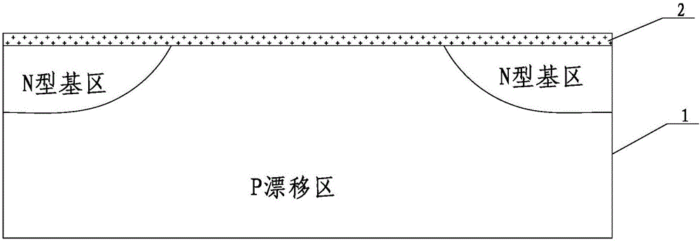
[0030] Step 2), remove the remaining photoresist on the oxide layer 2, and form the required N-type base junction depth on the upper surface of the epitaxial layer 1 after high-temperature annealing, such as figure 2 shown;
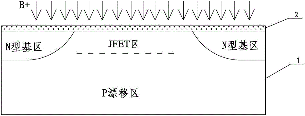
[0031] Step 3), perform comprehensive low-dose implantation of boron impurities (B+) on the oxide layer 2, and form a JFET region between the junction depths of the N-type base region, such as image 3 As shown, the comprehensive low-dose implantation o...
PUM
 Abstract
Description
Claims
Application Information


