Photoelectronic device, semiconductor substrate and manufacturing method thereof

A manufacturing method and semiconductor technology, applied in semiconductor devices, electrical components, circuits, etc., can solve the problems of narrow absorption band and affect the wide application of silicon-based photodetectors, and achieve the effect of broadening the absorption band

Inactive Publication Date: 2016-11-09
CHANGCHUN INST OF OPTICS FINE MECHANICS & PHYSICS CHINESE ACAD OF SCI
View PDF4 Cites 11 Cited by
  • Summary
  • Abstract
  • Description
  • Claims
  • Application Information

AI Technical Summary

Problems solved by technology

[0006] In view of this, the present invention provides an optoelectronic device, a semiconductor substrate and a manufacturing method thereof, to solve

Method used


Image

  • Photoelectronic device, semiconductor substrate and manufacturing method thereof
  • Photoelectronic device, semiconductor substrate and manufacturing method thereof
  • Photoelectronic device, semiconductor substrate and manufacturing method thereof

Examples


Embodiment Construction

[0042] The following will clearly and completely describe the technical solutions in the embodiments of the present invention with reference to the accompanying drawings in the embodiments of the present invention. Obviously, the described embodiments are only some, not all, embodiments of the present invention. Based on the embodiments of the present invention, all other embodiments obtained by persons of ordinary skill in the art without making creative efforts belong to the protection scope of the present invention.

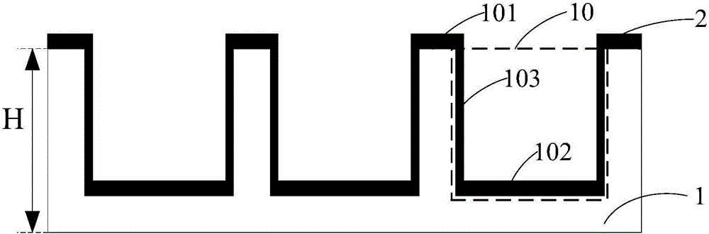
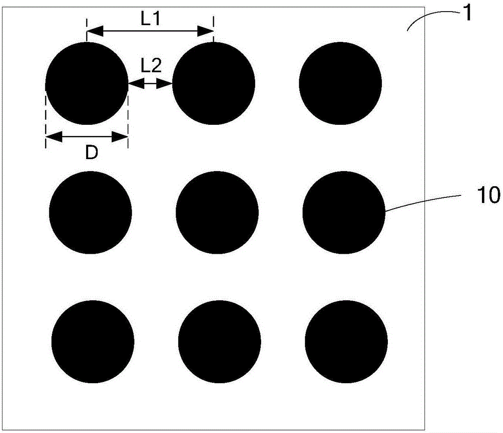
[0043] An embodiment of the present invention provides a semiconductor substrate, such as figure 1 As shown, the semiconductor substrate includes a silicon substrate 1 and a metal layer 2 located on the first surface of the silicon substrate 1, and the first surface of the silicon substrate 1 has a plurality of grooves 10, such as figure 2 As shown, these grooves 10 are preferably arranged periodically, of course, the present invention is not limited thereto....


PUM

PropertyMeasurementUnit
Diameteraaaaaaaaaa
Spacingaaaaaaaaaa
Depthaaaaaaaaaa

Abstract

The invention provides a photoelectronic device, a semiconductor substrate and a manufacturing method thereof. The semiconductor substrate comprise a silicon substrate and a metal layer positioned on the first surface of the silicon surface, wherein a plurality of grooves are formed in the first surface of the silicon substrate; and the areas among the grooves as well as the bottom surfaces and side walls of the grooves are covered with the metal layer. The grooves and the metal layer on the surfaces of the grooves can serve as U-shaped waveguides, multiple modes of surface plasma polariton excitation exist in the U-shaped waveguides, and the absorption band of the semiconductor substrate can be widened through the multiple modes of surface plasma polariton excitation, so that silicon substrate photoelectronic devices and silicon substrate photoelectric detectors are widely applied.

Description

technical field [0001] The invention relates to the field of optoelectronic technology, more specifically, to an optoelectronic device, a semiconductor substrate and a manufacturing method thereof. Background technique [0002] A photodetector is an optoelectronic device that converts light radiation energy into electrical energy, and it has a wide range of applications in various fields of military and national economy. For example, photodetectors with a response range in the visible or near-infrared band can be used for ray measurement and detection, industrial automatic control, and photometry; photodetectors with a response range in the infrared band can be used for missile guidance, infrared thermal imaging, and infrared remote sensing Wait. [0003] Although most of the existing photodetectors are made of silicon material as the substrate, due to the wide band gap of silicon material, the detection band of the photodetector is mainly concentrated in the visible light ...

Claims


Application Information

Patent Timeline
IPC IPC(8): H01L31/0392H01L31/0236H01L31/09H01L31/18
CPCH01L31/02363H01L31/0392H01L31/09H01L31/18Y02P70/50
Inventor 高劲松刘小翼杨海贵李强王延超李资政王笑夷
Owner CHANGCHUN INST OF OPTICS FINE MECHANICS & PHYSICS CHINESE ACAD OF SCI
Why Eureka
Try Eureka