Preparation method of back-illuminated image sensor

An image sensor, back-illuminated technology, applied in the field of image sensors, can solve the problem of weakening blue light quantum efficiency, achieve the effect of improving quantum efficiency and making up for the limitation of ion implantation process

Active Publication Date: 2016-11-16
OMNIVISION TECH (SHANGHAI) CO LTD
View PDF2 Cites 6 Cited by
  • Summary
  • Abstract
  • Description
  • Claims
  • Application Information

AI Technical Summary

Problems solved by technology

In order to improve the quantum efficiency of infrared light, the overall thickness of the semiconductor substrate is often increased in the prior art, however, this will weaken the quantum efficiency of blue light

Method used


Image

  • Preparation method of back-illuminated image sensor
  • Preparation method of back-illuminated image sensor
  • Preparation method of back-illuminated image sensor

Examples


preparation example Construction

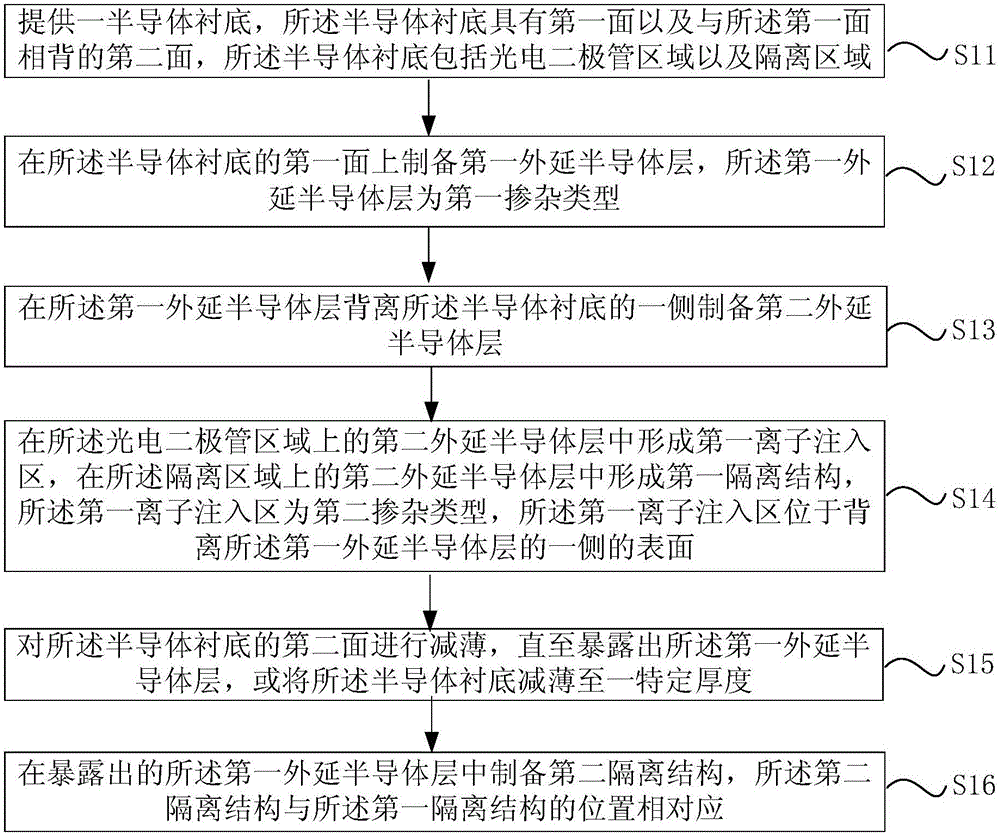
[0031] According to the above research, the present invention provides a method for preparing a back-illuminated image sensor, providing a method for preparing a back-illuminated image sensor, such as figure 1 shown, including the following steps:

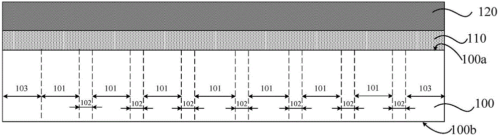
[0032] Step S11, providing a semiconductor substrate, the semiconductor substrate has a first surface and a second surface opposite to the first surface, the semiconductor substrate includes a photodiode region and an isolation region;

[0033] Step S12, preparing a first epitaxial semiconductor layer on the first surface of the semiconductor substrate, the first epitaxial semiconductor layer being of a first doping type;

[0034] Step S13, preparing a second epitaxial semiconductor layer on the side of the first epitaxial semiconductor layer away from the semiconductor substrate;

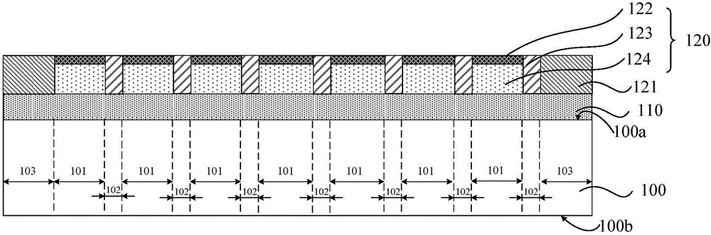
[0035] Step S14, forming a first ion implantation region in the second epitaxial semiconductor layer on the photodiode region, forming a first isolati...


PUM

PropertyMeasurementUnit
Doping concentrationaaaaaaaaaa
Thicknessaaaaaaaaaa
Doping concentrationaaaaaaaaaa

Abstract

The invention discloses a preparation method of a back-illuminated image sensor. The preparation method comprises the following steps: providing a semiconductor substrate, wherein the semiconductor substrate is provided with a first side and a second side opposite to the first side; preparing a first epitaxial semiconductor layer and a second epitaxial semiconductor layer on the first side of the semiconductor substrate; forming first ion injection regions in the second epitaxial semiconductor layer in photodiode regions and forming first isolation structures in the second epitaxial semiconductor layer in isolation regions, wherein the first ion injection regions are arranged on the surface of the side deviating from the first epitaxial semiconductor layer; thinning the second side of the semiconductor substrate until the first epitaxial semiconductor layer is exposed; preparing second isolation structures in the exposed first epitaxial semiconductor layer. The preparation method of the back-illuminated image sensor can achieve the effects of improving the quantum efficiency (QE) of infrared light and also improving the QE of blue light.

Description

technical field [0001] The invention relates to the technical field of image sensors, in particular to a method for preparing a back-illuminated image sensor. Background technique [0002] With the rapid development of the mobile Internet, people's demand for smart terminals is increasing, and image sensors, known as the "eyes" of smart terminals, have also ushered in unprecedented development space. The traditional CCD (Charge-coupled Device, charge-coupled device) image sensor is limited in high-performance digital cameras due to its high power consumption; Moreover, it is easy to be compatible with existing semiconductor processes, and the production cost is low, which makes CMOS image sensors occupy half of the image sensor market. [0003] CIS is divided into two technologies: front-illuminated and back-illuminated. Front-illuminated refers to the technology in which light enters the photodiode (PD) through the metal interconnection layer gap on the front of the chip. ...

Claims


Application Information

Patent Timeline
IPC IPC(8): H01L27/146H01L21/822
CPCH01L21/822H01L27/146H01L27/1464H01L27/14643H01L27/14683H01L27/14689
Inventor 刘远良李全宝
Owner OMNIVISION TECH (SHANGHAI) CO LTD
Why Eureka
Try Eureka