P electrode structure of LED chip, LED chip structure and manufacturing method therefor

A technology of LED chip and electrode structure, applied in circuits, electrical components, semiconductor devices, etc., can solve the problem of limiting the improvement of chip brightness, and achieve the effect of improving brightness, improving visible light reflectivity, and simple manufacturing process

Active Publication Date: 2016-11-16
XIAMEN CHANGELIGHT CO LTD
View PDF4 Cites 8 Cited by
  • Summary
  • Abstract
  • Description
  • Claims
  • Application Information

AI Technical Summary

Problems solved by technology

However, the introduction of Cr also brings a strong light absorption effect, resulting in the reflectivity of the entire reflective electrode being only about 70%, which limits the improvement of chip brightness.

Method used


Image

  • P electrode structure of LED chip, LED chip structure and manufacturing method therefor
  • P electrode structure of LED chip, LED chip structure and manufacturing method therefor

Examples


Embodiment Construction

[0028] In order to further explain the technical solution of the present invention, the present invention will be described in detail below through specific examples.

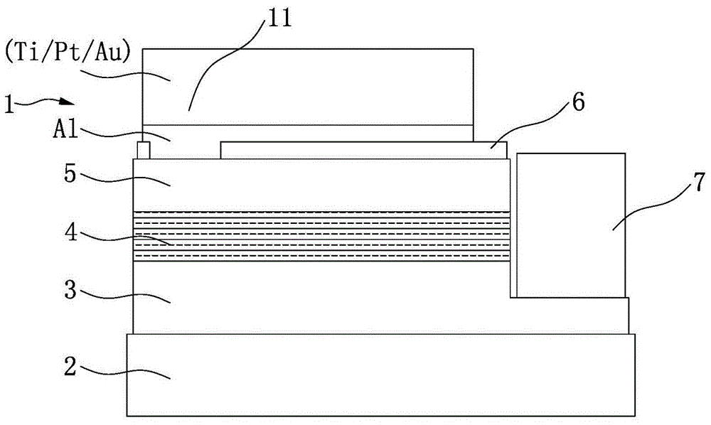
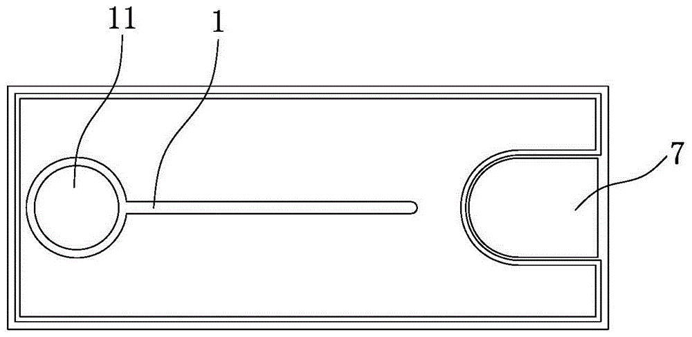
[0029] Such as figure 1 As shown, which includes a P electrode structure of an LED chip disclosed in the present invention, the P electrode 1 structure is composed of multiple layers of metal, which are Al, Ti, Pt and Au from bottom to top.

[0030] Such as Figure 1-2 Shown is an LED chip structure disclosed by the present invention, including a substrate 2 , an N-type layer 3 , an active layer 4 , a P-type layer 5 , an ITO transparent conductive layer 6 , a P electrode 1 and an N electrode 7 . Wherein the N-type layer 3 is an N-GaN layer, and the P-type layer 5 is a P-GaN layer.

[0031] An N-type layer 3 , an active layer 4 and a P-type layer 5 are sequentially formed on a substrate 2 , and the N-type layer 3 is connected to an N electrode 7 . The ITO transparent conductive layer 6 is formed on the P-type...


PUM


Abstract

The invention discloses a P electrode structure of an LED chip, an LED chip structure and a manufacturing method therefor. The P electrode is formed by multiple layers of metals, wherein Al is at the lowest layer; the LED chip structure comprises a substrate, an N type layer, an active layer, P type layer, an ITO transparent conductive layer, a P electrode and an N electrode; the N type layer, the active layer and the P type layer are formed on the substrate in sequence; the N type layer is connected with the N electrode; the ITO transparent conductive layer is formed on the P type layer; the P electrode is formed on the ITO transparent conductive layer, wherein the metal Al is arranged on the lowest layer of the P electrode; and Al is heated and permeated to the ITO transparent conductive layer, so that schottky contact is formed between the ITO transparent conductive layer and the P type layer. According to the P electrode structure of the LED chip, the LED chip structure and the manufacturing method therefor, the luminous reflectance of the electrode is improved; the luminance of the LED chip is improved; and the manufacturing process for the LED chip is simpler.

Description

technical field [0001] The invention relates to the technical field of LEDs, in particular to a P electrode structure of an LED chip, an LED chip structure and a manufacturing method thereof. Background technique [0002] The conventional chip structure of LED includes the following five steps: Mesa, CB, TCL, Pad, PV. Among them, the CB (current blocking) layer is often used as an insulating material such as silicon oxide or nitride. Although this type of material can form a very good insulating layer to achieve the purpose of current blocking, due to the limitation of the nature of the material itself, the CB layer is often broken during the chip packaging and wiring process, resulting in chip electrodes falling off. Phenomenon. [0003] Conventional front-mount LED chip electrodes are distributed on the front of the chip, which is the same as the light-emitting surface of the chip. Since the electrodes are opaque, they have a great impact on the quantum efficiency outsid...

Claims


Application Information

Patent Timeline
Patent Type & Authority Applications(China)
IPC IPC(8): H01L33/38H01L33/40H01L33/42H01L33/48H01L33/00
CPCH01L33/005H01L33/38H01L33/405H01L33/42H01L33/48H01L2933/0016
Inventor 邬新根张永陈凯轩李俊贤吴奇隆李小平陈亮刘英策魏振东周弘毅黄新茂蔡立鹤
Owner XIAMEN CHANGELIGHT CO LTD
Why Eureka
Try Eureka