PN junction

A PN junction and light doping technology, applied in the field of PN junction, can solve the problems of low modulation efficiency and high power consumption, and achieve the effect of improving modulation efficiency and reducing power consumption

Inactive Publication Date: 2016-11-23
ZTE CORP +1
View PDF4 Cites 8 Cited by
  • Summary
  • Abstract
  • Description
  • Claims
  • Application Information

AI Technical Summary

Problems solved by technology

However, this structure still has the problems o...

Method used


Image

  • PN junction
  • PN junction
  • PN junction

Examples


Embodiment Construction

[0034] In order to facilitate the understanding of those skilled in the art, the present invention will be further described below in conjunction with the accompanying drawings, which cannot be used to limit the protection scope of the present invention. It should be noted that, in the case of no conflict, the embodiments in the present application and various manners in the embodiments can be combined with each other.

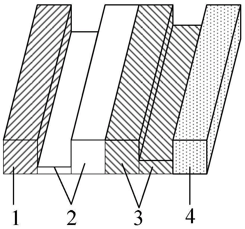
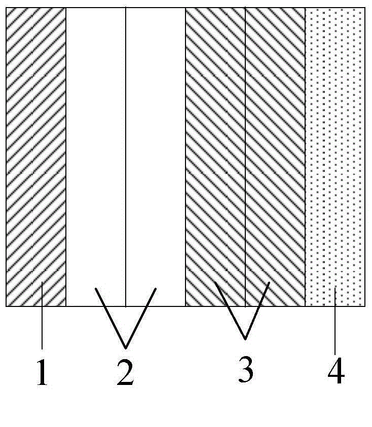
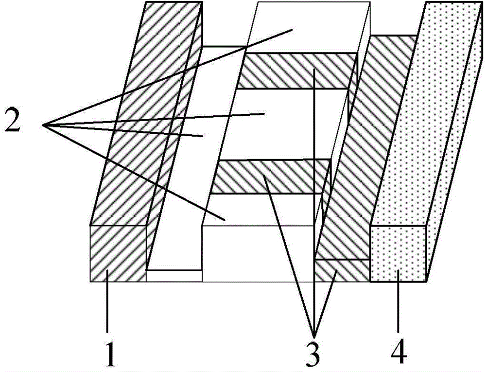
[0035] The invention proposes a PN junction, which at least includes: a lightly doped P region and a lightly doped N region connected to the lightly doped P region.

[0036] Among them, the lightly doped P region and the lightly doped N region form a novel interdigitated structure on the waveguide ridge region. Specifically, the lightly doped P regions and the lightly doped N regions are alternately distributed in the length direction of the waveguide ridge region, and the projection of the interface between the lightly doped P regions and the lightly doped N ...


PUM


Abstract

The invention discloses a PN junction. The PN junction at least comprises light-doped P regions and light-doped N regions connected with the light-doped P regions, wherein the light-doped P regions and the light-doped N regions are alternately distributed in the length direction of a waveguide ridge region, and the projection of the interface between the light-doped P regions and the light-doped N regions on the waveguide ridge region on the plane perpendicular to the interface is a broken line. By means of the scheme, modulation efficiency is improved, and power consumption is reduced.

Description

technical field [0001] The invention relates to semiconductor technology, in particular to a PN junction (P-N junction). Background technique [0002] Silicon-based optoelectronic integration uses silicon materials in the traditional microelectronics field as optoelectronic functional materials. It has the advantages of small size, low cost, easy integration, compatibility with complementary metal oxide (CMOS, Complementary MetalOxide Semiconductor) technology, and good stability. Ideal solution for optical communication, optical interconnect cost and power consumption bottlenecks. Silicon-based electro-optic modulator is a representative device in silicon-based optoelectronic integration, and has become a research hotspot in academia. [0003] Since silicon is a central inversion symmetric crystal, there is no linear electro-optic effect, and the high-order electro-optic effect is very weak, so light modulation can only be realized through other effects. Silicon-based ele...

Claims


Application Information

Patent Timeline
IPC IPC(8): G02F1/03
CPCG02F1/03
Inventor 周治平李田甜钟舫华锋王会涛
Owner ZTE CORP
Why Eureka
Try Eureka