

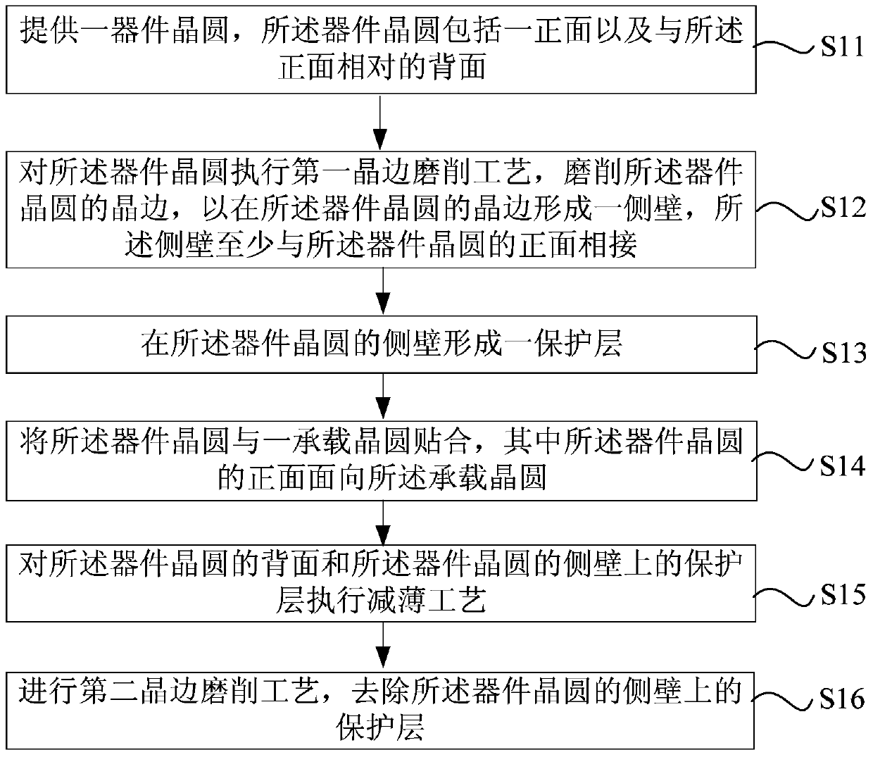
Wafer Thinning Methods
A technology of wafers and device wafers, which is applied in the field of wafer thinning, can solve problems affecting the process, and achieve the effect of avoiding peeling
- Summary
- Abstract
- Description
- Claims
- Application Information
AI Technical Summary
Problems solved by technology
Method used
Image

Examples
no. 1 example
[0046] see Figure 2-Figure 7 Specifically illustrate the wafer thinning method of the present invention, Figure 2-Figure 7 It is a schematic diagram of a cross-sectional structure of a wafer during the preparation process of the wafer thinning method according to the first embodiment of the present invention.
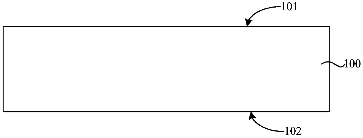
[0047] First, if figure 2 As shown, step S11 is performed to provide a device wafer 100 , and the device wafer 100 includes a front side 101 and a back side 102 opposite to the front side 101 . The front side 101 is prepared with device structures, such as active regions, gate structures, interconnect structures, and the like. The back surface 102 has a base material, such as a semiconductor material such as monocrystalline silicon.
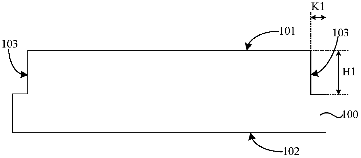
[0048] Then proceed to step S12, such as image 3 As shown, a first edge grinding process is performed on the device wafer 100 to grind the edge of the device wafer 100 to form a sidewall 103 at the edge of the device wafer 100 , t...
no. 2 example
[0060] see Figure 8-Figure 11 ,in, Figure 8-Figure 11 It is a schematic diagram of a cross-sectional structure of a wafer during the preparation process of the wafer thinning method according to the second embodiment of the present invention. exist Figure 8-Figure 11 , the reference numerals indicate the same Figure 2-Figure 7 The same expression is the same structure as the first embodiment. The method of the second embodiment is basically the same as the method of the first embodiment, the difference is that in step S13, as Figure 8 As shown, the protective layer 220 does not cover the front surface 101 of the device wafer 100 , and a covering layer 221 is formed on the front surface 101 of the device wafer 100 to protect the front surface 101 of the device wafer 100 . Preferably, the protective layer 120 is made of oxide, such as silicon oxide or silicon oxycarbide, which can well protect the interconnection structure at the sidewall 103 and is easily removed in st...
PUM
| Property | Measurement | Unit |
|---|---|---|
| thickness | aaaaa | aaaaa |
Abstract
Description
Claims
Application Information