MOS transistor forming method

A technology of MOS transistors and transistors, applied in semiconductor/solid-state device manufacturing, electrical components, circuits, etc., can solve the problems of poor performance and reliability of MOS transistors, reduce junction capacitance, suppress hot carrier injection effects and strike wear effect, performance-enhancing effect

Active Publication Date: 2016-11-23
SEMICON MFG INT (SHANGHAI) CORP
View PDF4 Cites 5 Cited by
  • Summary
  • Abstract
  • Description
  • Claims
  • Application Information

AI Technical Summary

Problems solved by technology

[0003] MOS transistors formed with prior art techniques suffer from

Method used


Image

  • MOS transistor forming method
  • MOS transistor forming method
  • MOS transistor forming method

Examples


Embodiment Construction

[0033] The performance and reliability of the MOS transistors formed in the prior art are poor as the feature size is further reduced.

[0034] Figure 1 to Figure 4 It is a schematic cross-sectional structure diagram of the formation process of the MOS transistor in an embodiment of the present invention.

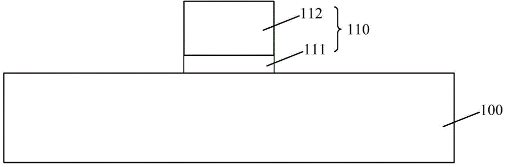
[0035] refer to figure 1 , providing a semiconductor substrate 100, forming a gate structure 110 on the surface of the semiconductor substrate 100, the gate structure 110 including a gate dielectric layer 111 on the surface of the semiconductor substrate 100 and a gate electrode layer 112 on the surface of the gate dielectric layer 111 .

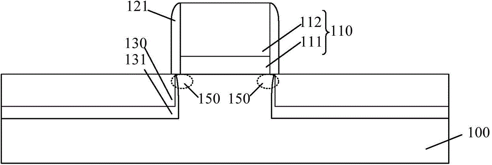
[0036] refer to figure 2 , forming an offset spacer 121 on the sidewall surface of the gate structure 110 .

[0037] Please still refer to figure 2 , using the offset spacer 121 and the gate structure 110 as a mask, perform lightly doped drain implantation to the semiconductor substrate 100 on both sides of the gate structure 110 ...


PUM

PropertyMeasurementUnit
Thicknessaaaaaaaaaa

Abstract

An MOS transistor forming method includes providing a semiconductor substrate whose surface is provided with a grid structure; performing first aureole injection on the semiconductor substrate on two sides of the grid structure by taking the grid structure as a mask; forming a shift side wall on the surface on two sides of the grid structure after first aureole injection; performing light-doped drain injection on the semiconductor substrate on the two sides of the grid structure by taking the grid structure with the shift side wall as the mask; and forming a source drain zone in the semiconductor substrate on the two sides of the grid structure. The MOS transistor forming method can improve performance and reliability of transistors.

Description

technical field [0001] The invention relates to the field of semiconductor manufacturing, in particular to a method for forming a MOS transistor. Background technique [0002] MOS (metal-oxide-semiconductor) transistor is one of the most important elements in modern integrated circuits. The basic structure of MOS transistor includes: semiconductor substrate; : a gate dielectric layer located on the surface of the semiconductor substrate and a gate electrode layer located on the surface of the gate dielectric layer; source and drain regions located on both sides of the gate structure. [0003] As the feature size is further reduced, the performance and reliability of MOS transistors formed by the prior art are poor. Contents of the invention [0004] The problem to be solved by the invention is to provide a method for forming a MOS transistor and improve the performance and reliability of the MOS transistor. [0005] In order to solve the above technical problems, the pre...

Claims


Application Information

Patent Timeline
IPC IPC(8): H01L21/336H01L21/266
Inventor 赵猛
Owner SEMICON MFG INT (SHANGHAI) CORP
Why Eureka
Try Eureka