semiconductor module
A semiconductor and interconnection layer technology, applied in the direction of semiconductor devices, semiconductor/solid-state device components, electric solid-state devices, etc., can solve problems such as unfavorable and affecting IGBT component gating
- Summary
- Abstract
- Description
- Claims
- Application Information
AI Technical Summary
Problems solved by technology
Method used
Image
Examples
no. 1 example
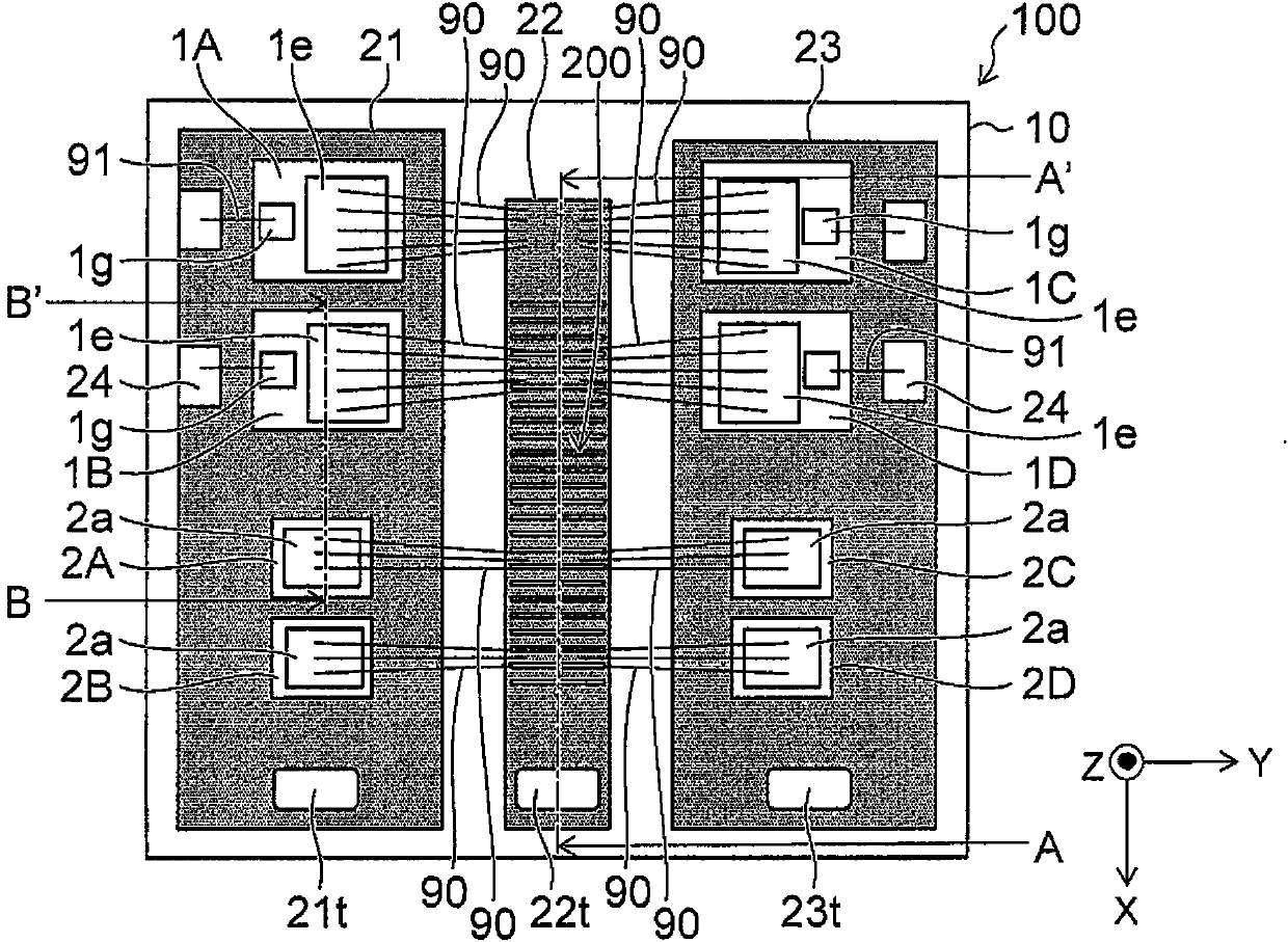
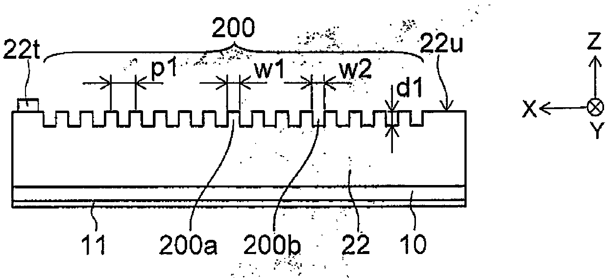
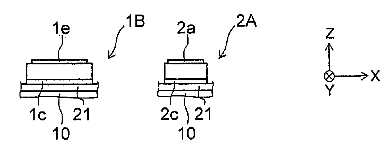
[0022] Figure 1A is a schematic plan view showing the semiconductor module according to the first embodiment, and Figure 1B and Figure 1C is a schematic cross-sectional view showing part of the semiconductor module according to the first embodiment.
[0023] In this article, along the Figure 1A The cross-section at the position taken by the line A-A' is shown in Figure 1B middle. along Figure 1A The cross-section at the position taken by the line BB' is shown in Figure 1C middle. In addition, three-dimensional coordinates are illustrated in the drawings to describe the arrangement relationship and dimensions of each component.
[0024] Figures 1A to 1C The semiconductor module 100 shown in includes a substrate 10, an interconnection layer 21 (first interconnection layer), an interconnection layer 22 (second interconnection layer), an interconnection layer 23 (third interconnection layer), a plurality of Semiconductor elements 1A and 1B (first semiconductor elemen...
no. 2 example
[0074] Figure 6A is a schematic plan view showing a semiconductor module according to the second embodiment, and Figure 6B is a schematic sectional view showing a part of the semiconductor module according to the second embodiment.
[0075] In this article, along the Figure 6A The cross-section at the position taken by the line C-C' is shown in Figure 6B middle.
[0076] In the semiconductor module 101 according to the second embodiment, the concavo-convex structure 201 is provided on the side surface 22 sw of the interconnection layer 22 . In some cases, the noise current is deflected to, for example, the side surface of the interconnection layer 22 . In this case, it is possible to effectively attenuate the S21 parameter using the concavo-convex structure 201 .
no. 3 example
[0078] Figure 7A is a schematic plan view showing a semiconductor module according to a third embodiment, and Figure 7B is a schematic sectional view showing a part of the semiconductor module according to the third embodiment.
[0079] In this article, along the Figure 7A The cross-section at the position taken by the line C-C' is shown in Figure 7B middle.
[0080] In the semiconductor module 102 according to the third embodiment, the concavo-convex structure 202 is provided on the surface of the interconnection layer 21 or the surface of the interconnection layer 23 . For example, the concave-convex structure 202 is provided on the side surface 21 sw of the interconnection layer 21 . In addition, a concavo-convex structure 202 is provided on the side surface 23sw of the interconnection layer 23 .
[0081] In the semiconductor module 102, the ground coplanar line consists of the interconnection layer 21 and the interconnection layer 23 provided on the substrate 10 a...
PUM
| Property | Measurement | Unit |
|---|---|---|
| Thickness | aaaaa | aaaaa |
Abstract
Description
Claims
Application Information
 - R&D Engineer
- R&D Manager
- IP Professional
- Industry Leading Data Capabilities
- Powerful AI technology
- Patent DNA Extraction
Browse by: Latest US Patents, China's latest patents, Technical Efficacy Thesaurus, Application Domain, Technology Topic, Popular Technical Reports.
© 2024 PatSnap. All rights reserved.Legal|Privacy policy|Modern Slavery Act Transparency Statement|Sitemap|About US| Contact US: help@patsnap.com


