Super junction power device and manufacturing method thereof

A power device and main junction technology, applied in the field of superjunction power devices and manufacturing, can solve the problems of reduced breakdown voltage, reduced ion concentration, and reduced surface breakdown voltage of superjunction power devices, etc.

Active Publication Date: 2016-11-23
FOUNDER MICROELECTRONICS INT
View PDF5 Cites 0 Cited by
  • Summary
  • Abstract
  • Description
  • Claims
  • Application Information

AI Technical Summary

Problems solved by technology

[0005] The technical problem to be solved by the present invention is that in the manufacturing process of the super junction power device in the prior art, the ion concentration on the surface of the P column area is reduced after the thermal process, ...

Method used


Image

  • Super junction power device and manufacturing method thereof
  • Super junction power device and manufacturing method thereof
  • Super junction power device and manufacturing method thereof

Examples


Embodiment 1

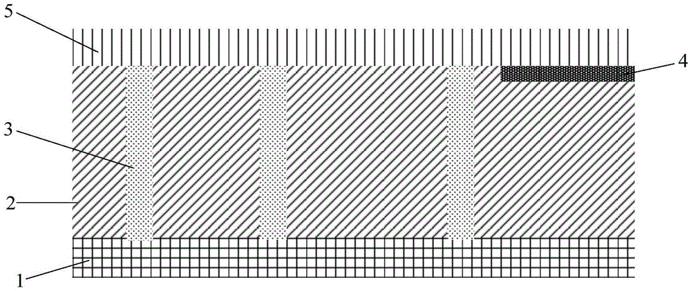
[0029] A super junction power device related to this embodiment includes an active region, a voltage divider region, a cutoff ring region, and a scribing track region. The voltage divider region is arranged on the periphery of the active region, and the cutoff ring region is arranged At the periphery of the active area, the scribe track area is arranged at the periphery of the stop ring area. The super junction power device will be described in detail below.

[0030] Such as figure 2 As shown, the voltage division area of ​​the super junction power device provided by the present invention includes a plurality of P pillars, and the density of the P pillars on the side close to the active area in the voltage division area is greater than that on the side close to the stop ring area The P column density; The P column density refers to the number of P columns per unit area of ​​the partial pressure region.

[0031] The super-junction power device of the present invention adopts P-pill...

Embodiment 2

[0043] The present invention also provides a method for a super junction power device, which includes the following steps:

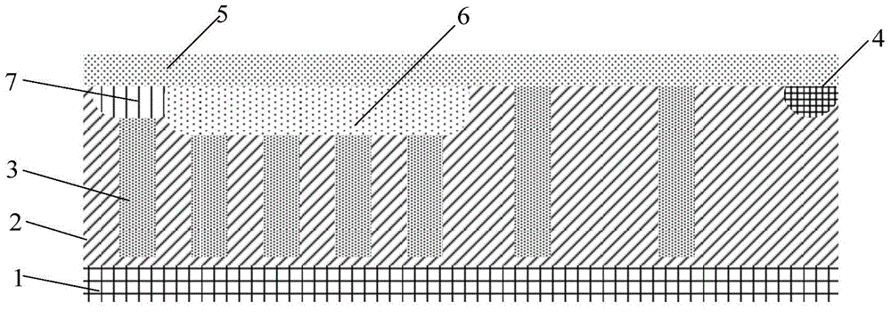
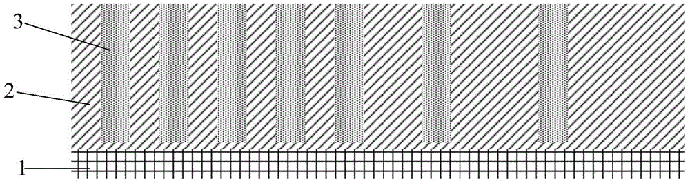
[0044] Step 1, as shown in Figure 3(a), a plurality of P pillars are formed in the partial pressure area on the surface of the silicon wafer. The P-pillar spacing on the side close to the active region in the voltage dividing region is the same, and the P-pillar spacing on the side close to the cut-off region gradually increases from the active region to the cut-off region;

[0045] In this embodiment, the ion concentration of each P column is the same, and the width is also the same. In this embodiment, using P-pillars with different distances in the voltage division region will reduce the surface electric field strength of the power device, thereby increasing the breakdown voltage;

[0046] Step two, as shown in FIG. 3(b), a shallow P-type implanted junction is implanted on the side close to the active region in the partial pressure region, and the shallow P...


PUM


Abstract

The invention relates to a super junction power device and a manufacturing method thereof. The super junction power device comprises an active region, a voltage-dividing region, a cutoff ring region and a scribing line region, wherein the voltage-dividing region is arranged on the periphery of the active region, the cutoff ring region is arranged on the periphery of the active region, the scribing line region is arranged on the periphery of the cutoff ring region, the voltage-dividing region comprises a plurality of P posts, and the density of the P posts at one side, close to the active region, of the voltage-dividing region is greater than that of the P posts at one side close to the cutoff ring region. The super junction power device terminal adopts the P posts with different distances in the voltage-dividing region, so that the intensity of a surface electrical field of the super junction power device is reduced, the breakdown voltage is increased, the influence of the an electrical field accumulated at the surface of an oxidation layer on the voltage-dividing region is eliminated, the area of the voltage-dividing region is reduced, the device performance is improved, and the device manufacturing cost is reduced.

Description

Technical field [0001] The invention relates to a power device, in particular to a super junction power device and a manufacturing method. Background technique [0002] Vertical double diffused field effect transistor (VDMOS for short) is a new type of power semiconductor device with rapid development and wide application. It introduces a super junction structure on the basis of ordinary vertical double diffused metal oxide semiconductors, so that it has high VDMOS input impedance, fast switching speed, high operating frequency, voltage control, good thermal stability, and simple drive circuit advantage. Its two poles are on both sides of the device, so that the current flows vertically inside the device, which increases the current density, improves the rated current, and has a smaller on-resistance per unit area. It is a very versatile power device. [0003] Field limiting loop technology is one of the most commonly used voltage divider structures in power devices. The process...

Claims


Application Information

Patent Timeline
IPC IPC(8): H01L29/78H01L29/06H01L21/336
Inventor 李理马万里赵圣哲
Owner FOUNDER MICROELECTRONICS INT
Why Eureka
Try Eureka