Super-junction power device and fabrication method thereof

A technology of a power device and a manufacturing method, applied in the field of superjunction power devices and their manufacturing, can solve the problems affecting the surface breakdown strength, the reduction of the ion concentration, the reduction of the breakdown voltage, etc., so as to reduce the area of ​​the partial pressure region and improve the ion concentration. , the effect of electric field spike enhancement

Inactive Publication Date: 2016-11-23
PEKING UNIV FOUNDER GRP CO LTD +1
View PDF4 Cites 1 Cited by
  • Summary
  • Abstract
  • Description
  • Claims
  • Application Information

AI Technical Summary

Problems solved by technology

There are often some impurities in the surface oxide layer of this structure, which leads to the generation of interface charges on the surface, which will have a great impact on the surface potential of super junction power devices, affect the voltage division effect, and reduce the breakdown voltage
At the same time, during the manufacturing process, the ion concentration on the surface of the P-pillar area will decrease after multiple thermal processes of the super-junction power device, which will affect the surface breakdown strength, reduce the breakdown voltage of the super-junction power device, and affect the device performance.

Method used


Image

  • Super-junction power device and fabrication method thereof
  • Super-junction power device and fabrication method thereof
  • Super-junction power device and fabrication method thereof

Examples


Embodiment 1

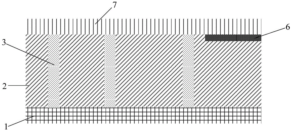
[0029] Such as figure 1 As shown, the super junction power device of this embodiment includes an active area, a voltage dividing area, a stop ring area and a scribe lane area, the voltage dividing area is set on the periphery of the active area, and the stop ring area is set on the periphery of the active region, the scribe lane region is disposed on the periphery of the stop ring region,

[0030] The voltage dividing region includes a plurality of P pillars 3 with the same pitch, and the width of the P pillars 3 gradually decreases from the active region to the stop ring.

[0031] The voltage division region of the super junction power device adopts P columns 3 with different widths to reduce the surface electric field intensity of the power device, so that the concentration of P-type ions per unit area changes, thereby increasing the surface ion concentration in the voltage division region, reducing The influence of the electric field accumulated on the surface of the oxide...

Embodiment 2

[0040] The present invention also provides a method for manufacturing a super junction power device, comprising the following steps:

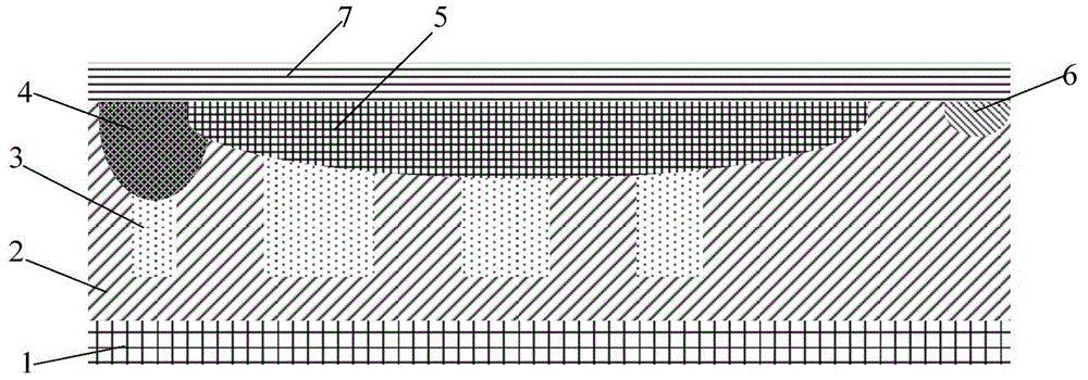
[0041] Step 1, as shown in Figure 3 (a), a substrate is provided, the substrate includes a silicon wafer 1 and an N-type epitaxial layer 2, and a P pillars, wherein the width of the P pillars 3 in the active region is equal, and the width of the P pillars 3 in the partial pressure region gradually decreases from the active region to the direction of the stop ring region; the ion concentration of the P pillars 3 is the same .

[0042] The manufacturing method of the present invention adopts P pillars 3 with different widths in the partial pressure region to reduce the surface electric field intensity of the power device, so that the P-type ion concentration per unit area changes, thereby increasing the surface ion concentration in the partial pressure region and reducing the electric field intensity of the power device. The influence of the ele...


PUM


Abstract

The invention relates to a super-junction power device and a fabrication method thereof. The super-junction power device comprises an active region, a voltage division region, a cutoff ring region and a scribing channel region, wherein the voltage division region is arranged at the periphery of the active region, the cutoff ring region is arranged at the periphery of the active region, the scribing channel region is arranged at the periphery of the cutoff ring region, a plurality of P posts at the same interval are formed in the voltage division region, and the widths of the P posts in a direction from the active region to the cutoff ring region are gradually reduced. With the super-junction power device provided by the invention, the influence of an electric field accumulated on the surface of an oxide layer on the voltage division region can be reduced, meanwhile, the surface breakdown strength of the super-junction power device is improved, the area of the voltage division region is reduced, the performance of the device is improved, and the manufacturing cost of the device is reduced.

Description

technical field [0001] The invention relates to a power device, in particular to a super junction power device and a manufacturing method thereof. Background technique [0002] Vertical Double Diffused Field Effect Transistor (VDMOS for short) is a new power semiconductor device with rapid development and wide application. It introduces a super junction (Super junction) structure on the basis of ordinary vertical double-diffused metal oxide semiconductors, so that it has VDMOS high input impedance, fast switching speed, high operating frequency, voltage control, good thermal stability, and simple drive circuit. advantage. Its two poles are on both sides of the device, so that the current flows vertically inside the device, increasing the current density, improving the rated current, and the on-resistance per unit area is also small. It is a very versatile power device. [0003] Field limiting ring technology is one of the most commonly used voltage divider structures in po...

Claims


Application Information

Patent Timeline
Patent Type & Authority Applications(China)
IPC IPC(8): H01L29/78H01L29/06H01L21/336
CPCH01L29/7811H01L29/0634H01L29/66712
Inventor 李理马万里赵圣哲
Owner PEKING UNIV FOUNDER GRP CO LTD
Why Eureka
Try Eureka