Method for Junction Staining of Transmission Electron Microscopy Samples

An electron microscope and sample technology, applied in the preparation of test samples, etc., can solve problems such as analysis failure, improve accuracy and success rate, and avoid damage

Active Publication Date: 2019-07-23
SHANGHAI HUALI MICROELECTRONICS CORP
View PDF9 Cites 0 Cited by
  • Summary
  • Abstract
  • Description
  • Claims
  • Application Information

AI Technical Summary

Problems solved by technology

This creates a problem where the analysis fails when the defect is located exactly in the cut-out area

Method used


Image

  • Method for Junction Staining of Transmission Electron Microscopy Samples
  • Method for Junction Staining of Transmission Electron Microscopy Samples
  • Method for Junction Staining of Transmission Electron Microscopy Samples

Examples


Embodiment Construction

[0024] In order to make the content of the present invention clearer and easier to understand, the content of the present invention will be described in detail below in conjunction with specific embodiments and accompanying drawings.

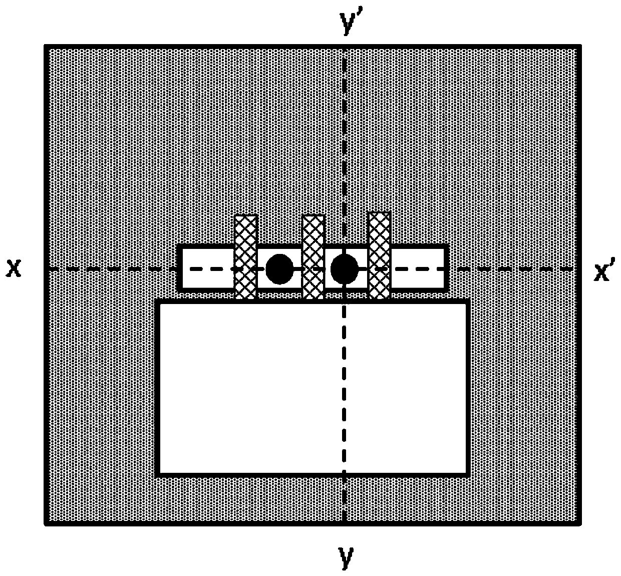
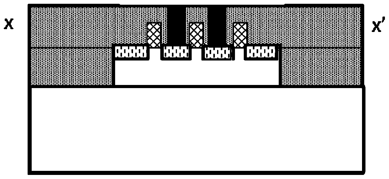
[0025] Figure 1 to Figure 12 Each step of the method for staining a transmission electron microscope sample junction according to a preferred embodiment of the present invention is schematically shown.

[0026] Such as Figure 1 to Figure 12 Shown, according to the method for transmission electron microscope sample junction staining of preferred embodiment of the present invention comprises:

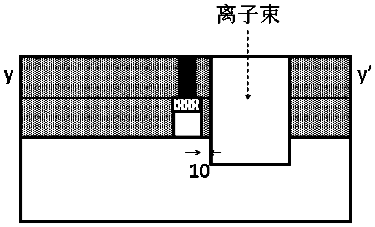
[0027] First step: using a focused ion beam to cut the first side of the sample to a SiO laterally at a first predetermined thickness of 10 from the junction to be measured 2 at the location;

[0028] Preferably, the first predetermined thickness 10 is 10-30 nm.

[0029] The resulting structure is as figure 1 top view of figure 2 shown along the f...


PUM

PropertyMeasurementUnit
thicknessaaaaaaaaaa

Abstract

The invention provides a method for transmission electron microscope sample node dyeing. The method comprises the steps that a first side face of a sample is cut to the position of SiO2 a first preset thickness away from a to-be-detected node laterally; a first chemical reagent is used for removing whole remaining SiO2 on the first side face; a second chemical reagent is used for removing silicon doped in the to-be-detected node; a second side face of a transmission electron microscope sample is cut, a transmission electron microscope sample sheet is formed, ion beams do not directly cut Si, and SiO2 a second preset thickness away from the to-be-detected node is reserved laterally.

Description

technical field [0001] The invention relates to the field of integrated circuit analysis, and more specifically, the invention relates to a method for staining a sample of a transmission electron microscope. Background technique [0002] Transmission electron microscopes are widely used in various fields including integrated circuit analysis and are increasingly important, especially in the analysis of tiny defects, which play an irreplaceable role. [0003] There are many kinds of defects that can cause chip failure. Among them, the most difficult to analyze is the very tiny nanoscale doping anomaly. This type of defect cannot be observed by conventional analysis methods such as SEM and transmission electron microscope. At present, the only effective one is Junction staining method using transmission electron microscopy. [0004] The conventional sample preparation process for junction staining is to process the plane of the chip sample to be tested close to the target lay...

Claims


Application Information

Patent Timeline
Patent Type & Authority Patents(China)
IPC IPC(8): G01N1/28
Inventor 陈强陈胜
Owner SHANGHAI HUALI MICROELECTRONICS CORP
Why Eureka
Try Eureka