This helps you quickly interpret patents by identifying the three key elements:
Problems solved by technology
Method used
Benefits of technology
Problems solved by technology
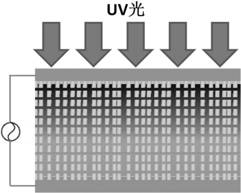
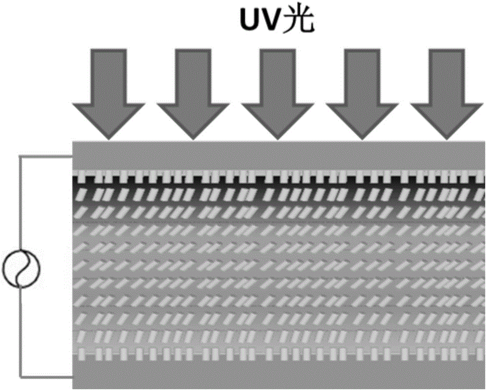
The larger the number of pixels per inch (PPI), the smaller the opening area of the thin film transistor (TFT), the smaller the light transmittance, the smaller the pretilt angle of the liquid crystal, and the risk of poor liquid crystal diffusion, such as figure 2 ; The smaller the number of pixels per inch (PPI), the larger the opening area of the thin film transistor (TFT), the larger the light transmittance, the larger the pretilt angle of the liquid crystal, and the risk of broken bright spots, such as image 3
Method used
Image
Click on the blue label to locate the original text in one second.
Reading with bidirectional positioning of images and text.
Examples
specific Embodiment approach 1
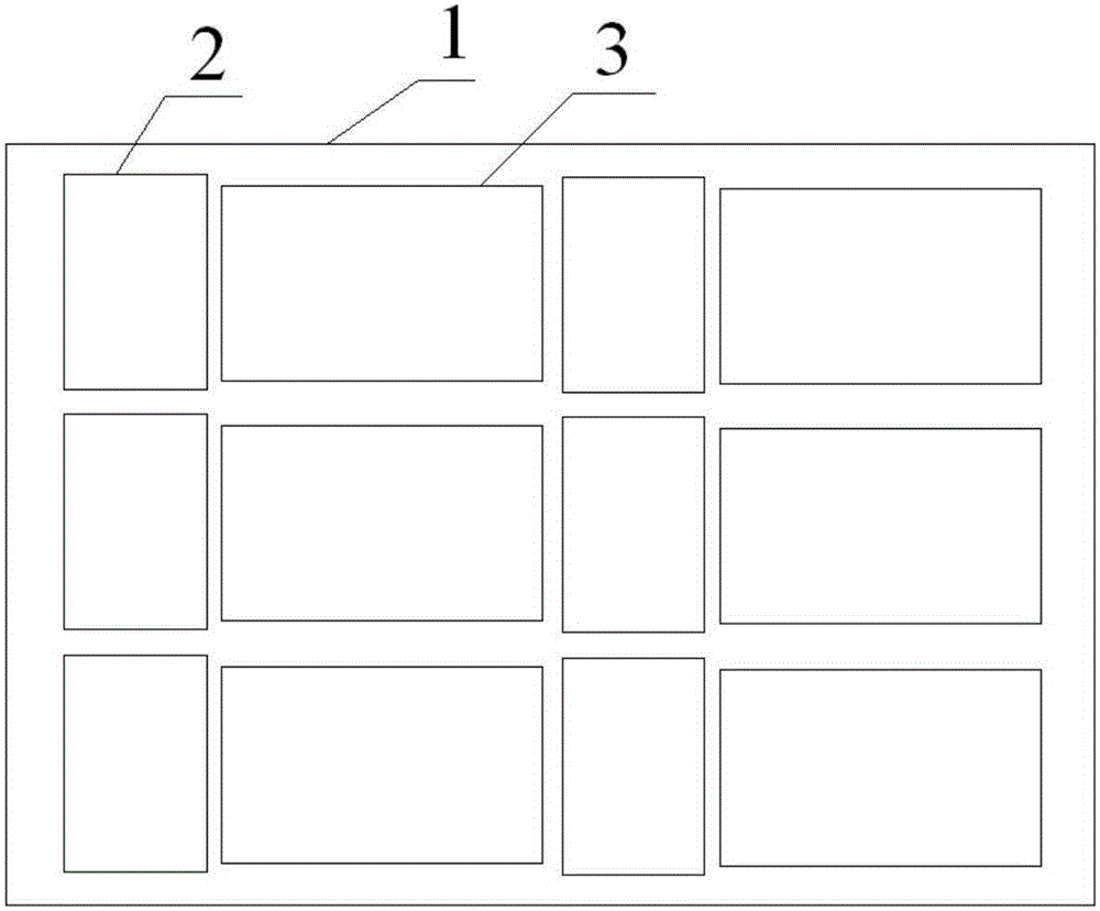
[0055] Specific implementation mode one: combine Figure 4 , Figure 5 , Image 6 , Figure 7 Describe this embodiment mode, a device for improving the optical alignment of a sleeve panel in this embodiment mode, including a sleeve cut substrate 1, N-row chip one 2, N-row chip two 3, and is characterized in that it also includes a photomask 4;
[0056] The N-row chips one (2) and the N-row chips two (3) are arranged alternately and sequentially to form an alternate arrangement structure, and are installed on the nesting substrate 1;
[0057] The area of the chip two 3 is greater than the area of the chip one 2;
[0058] The photomask 4 is used to cover N row chip one (2) and N row chip two 3, so that ultraviolet light passes through the photomask to irradiate N row chip one 2 and N row chip two 3;
[0059] Said N is a positive integer.
specific Embodiment approach 2
[0060] Embodiment 2: This embodiment is different from Embodiment 1 in that: the number of pixels per inch (PPI) in the operable area (AA) of the N columns of chips (Chip) with different areas is different.
[0061] The difference in the number of pixels per inch (PPI) affects the size of the liquid crystal pre-tilt angle.
[0062] Other steps and parameters are the same as those in Embodiment 1.
specific Embodiment approach 3
[0063] Specific embodiment three: the difference between this embodiment and specific embodiment one or two is:
[0064] The pixels include:
[0065] a first alignment film formed on the first substrate and a second alignment film formed on the second substrate and facing the first alignment film;
[0066] A plurality of adjacent domains, each of which includes a normal luminance area and a domain boundary area, each domain boundary area defining a partial area between adjacent domains.
[0067] Figure 9 is a perspective view of a partial cross-section of a liquid crystal display panel showing the combination of a liquid crystal layer and a substrate with a polarizer and an alignment film. refer to Figure 9 The liquid crystal display panel 5 has a first substrate 6 , a second substrate 10 and a liquid crystal layer 14 interposed between the first substrate 6 and the second substrate 10 .
[0068] like Figure 9 As shown, the first polarizer 8 is fabricated in the form o...
PUM
Property
Measurement
Unit
wavelength
aaaaa
aaaaa
wavelength
aaaaa
aaaaa
Abstract
The invention discloses a device for improving the optical orientation of a sleeve cutting type panel. The device aims to overcome the defect of the prior art that product quality is affected. The device comprises a sleeve cutting type substrate (1), first N rows of chips (2) and second N rows of chips (3) and is characterized by further comprising a photomask (4), the first N rows of chips (2) and the second N rows of chips (3) are arranged alternately and sequentially to form an alternate arrangement structure and installed on the sleeve cutting type substrate (1), the area of the second chips (3) is larger than that of the first chips (2), the photomask (4) is used for covering the first N rows of chips (2) and the second N rows of chips (3) to enable ultraviolet light to irradiate on the first N rows of chips (2) and the second N rows of chips (3) through the photomask, and N is a positive integer. The device is used for manufacturing thin film transistorliquid crystal displays.
Description
technical field [0001] The invention relates to the field of display technology, in particular to a device for improving the light alignment of a sleeve cut panel. Background technique [0002] The liquid crystal display module includes: a liquid crystal display panel for displaying an image on the liquid crystal display panel by changing an arrangement of liquid crystal molecules in the liquid crystal layer according to an electric field generated in the liquid crystal layer; a backlight assembly for supplying light to the liquid crystal display panel; and a case, The liquid crystal display panel and the backlight assembly are fixed in the case. [0003] A liquid crystal display panel includes a liquid crystal layer, a pair of substrates with the liquid crystal layer interposed therebetween, and a pair of polarizers attached to the outside of the substrates. Images displayed on a liquid crystal display panel are expected to have the same display quality no matter which dir...
Claims
Application Information
Patent Timeline
Application Date:The date an application was filed.
Publication Date:The date a patent or application was officially published.
First Publication Date:The earliest publication date of a patent with the same application number.
Issue Date:Publication date of the patent grant document.
PCT Entry Date:The Entry date of PCT National Phase.
Estimated Expiry Date:The statutory expiry date of a patent right according to the Patent Law, and it is the longest term of protection that the patent right can achieve without the termination of the patent right due to other reasons(Term extension factor has been taken into account ).
Invalid Date:Actual expiry date is based on effective date or publication date of legal transaction data of invalid patent.

