GOA (Gate Driver On Array) circuit and liquid crystal display panel

An array substrate row and drive circuit technology, applied in nonlinear optics, instruments, optics, etc., can solve problems such as large circuit load, GOA circuit damage, alignment failure, etc., and achieve the effect of improving compatibility

Inactive Publication Date: 2016-12-07
SHENZHEN CHINA STAR OPTOELECTRONICS TECH CO LTD
View PDF6 Cites 15 Cited by
  • Summary
  • Abstract
  • Description
  • Claims
  • Application Information

AI Technical Summary

Problems solved by technology

[0005] For the existing GOA array substrate, at present, the liquid crystal alignment is carried out by means of the GOA circuit. Due to the large load of the circuit during liquid crystal alignment, it is easy to cause damage to the GOA circuit and alignment failure. At the same time, because it is different from the traditional alignment circuit, it is necessary to develop a new liquid crystal alignment fixture

Method used


Image

  • GOA (Gate Driver On Array) circuit and liquid crystal display panel
  • GOA (Gate Driver On Array) circuit and liquid crystal display panel
  • GOA (Gate Driver On Array) circuit and liquid crystal display panel

Examples


Embodiment Construction

[0029] The following descriptions of the various embodiments refer to the accompanying drawings to illustrate specific embodiments in which the invention may be practiced. The directional terms mentioned in the present invention, such as [top], [bottom], [front], [back], [left], [right], [inside], [outside], [side], etc., are only for reference The orientation of the attached schema. Therefore, the directional terms used are used to illustrate and understand the present invention, but not to limit the present invention. In the figures, structurally similar elements are denoted by the same reference numerals.

[0030] The present invention aims at the technical problems of the existing GOA circuit, which easily causes damage to the GOA circuit and failure of alignment due to the large circuit load during liquid crystal alignment, and this embodiment can solve this defect.

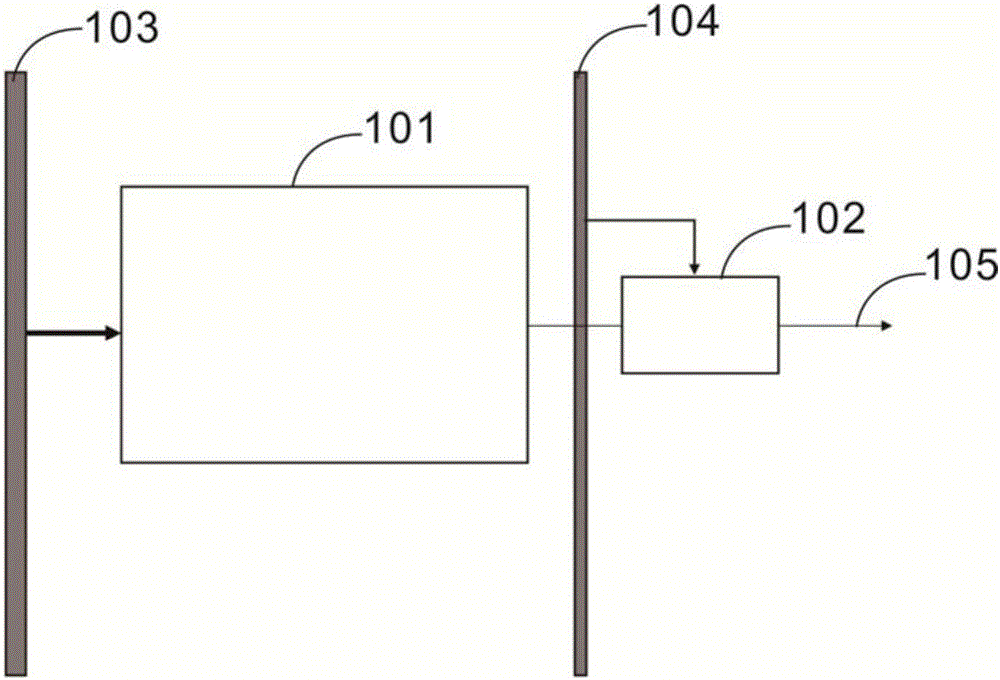
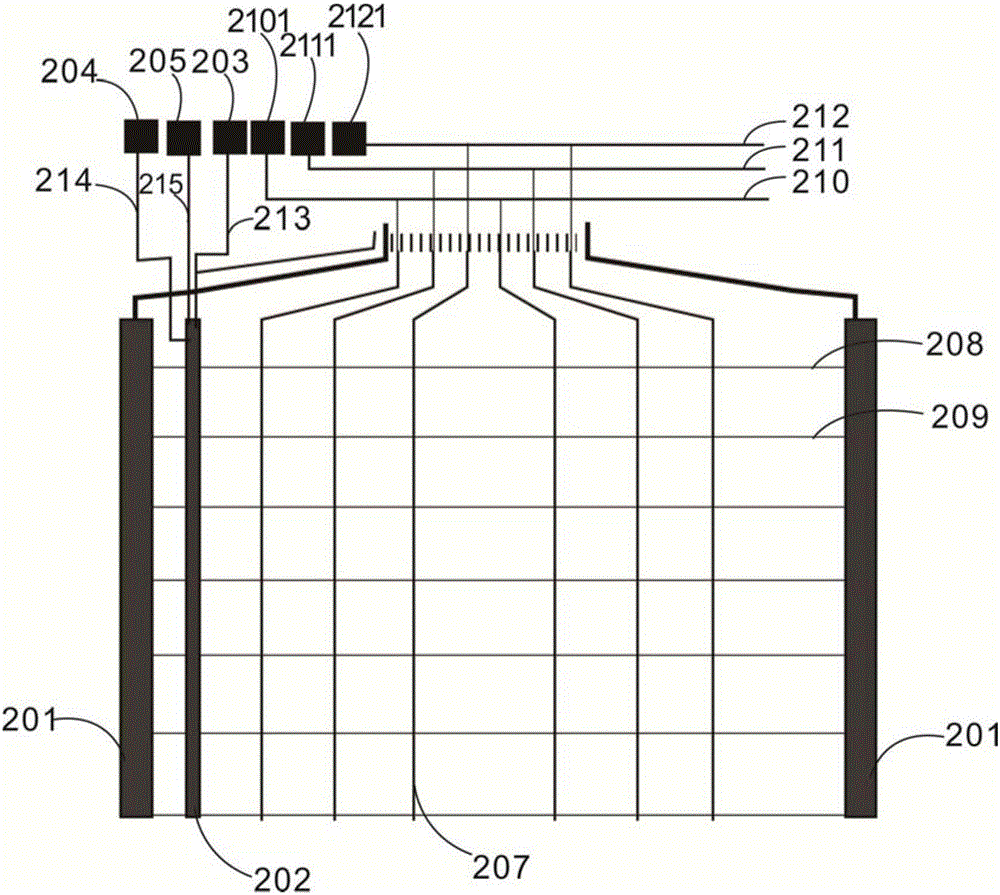
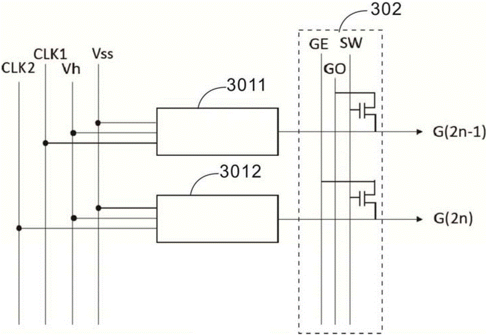
[0031] Such as figure 1 As shown, the array substrate row driving circuit includes a GOA circuit 101; ...


PUM


Abstract

The invention provides a GOA (Gate Driver On Array) circuit which comprises an alignment terminal region, a liquid crystal alignment circuit and a field effect transistor, wherein the alignment terminal region comprises a switching signal terminal, gate signal terminals and a data signal input terminal; the output end of the liquid crystal alignment circuit is connected with the alignment terminal region; the field effect transistor outputs an alignment voltage signal on a corresponding data line to a corresponding pixel electrode according to a gate electrode signal on a scanning line. The GOA circuit has the beneficial effects that by adding an alignment circuit at the output end of the GOA circuit and separating the GOA circuit from the alignment circuit, in the liquid crystal alignment process, the alignment circuit inputs testing signals to odd and even line gate lines so as to detect whether a rear end line is conducted; opening and closing of the alignment circuit are switched by changing a voltage of a switching signal line, so that the problems of damage to the GOA circuit and alignment failure, which are easy to caused due to a large circuit load in the liquid crystal alignment process, are avoided, and liquid crystal alignment efficiency and compatibility of a liquid crystal alignment jig are improved.

Description

technical field [0001] The invention relates to the technical field of liquid crystal display, in particular to an array substrate row driving circuit and a liquid crystal display panel with the array substrate row driving circuit. Background technique [0002] A liquid crystal display (LCD, Liquid Crystal Display) is one of the most widely used flat panel displays, and the LCD includes a pair of panels provided with field generating electrodes such as pixel electrodes and common electrodes and a liquid crystal (LC, Liquid Crystal) layer. When a voltage is applied to the field generating electrode to generate an electric field in the LC layer, the electric field determines the orientation of the LC molecules in the liquid crystal layer, thereby adjusting the polarization of light incident on the liquid crystal layer, allowing the LCD to display images. [0003] At present, a technology called Polymer Stabilized Vertical Alignment (PSVA) has been developed in the industry. T...

Claims


Application Information

Patent Timeline
Patent Type & Authority Applications(China)
IPC IPC(8): G02F1/1345G02F1/1337
CPCG02F1/13454G02F1/133707
Inventor 徐向阳
Owner SHENZHEN CHINA STAR OPTOELECTRONICS TECH CO LTD
Why Eureka
Try Eureka